Getting A Grip On Sapphire Etching

One common and effective route for increasing the bang-per-buck of the LED is to switch the foundation for the device from a flat sapphire substrate to one that has been etched to form a patterned surface. This alternative, known as patterned sapphire, is increasing in popularity because it delivers two key benefits to the makers of high-brightness LEDs: it increases the fraction of light emitted from the device, thanks to the controlled texture; and it leads to a lower density of defects within the film, thanks to growth on a three-dimensional landscape that spurs earlier coalescence of GaN epitaxial islands during MOCVD growth.
The downside of turning to patterned sapphire is that etching this material into useful patterns is not easy. There is a processing cost involved, and this must be low enough to not negate the benefit associated with increased LED performance.
Etching options
Two options are available for forming patterned sapphire: wet etching and dry etching. The former involves a combination of high pressures and a mixture of sulphuric and phosphoric acid, with very specialised equipment needed to ensure that work takes place in a safe manner. Etch rates can be relatively high, such as up to 1 mm per minute, but there is often the need for a hard mask. Unfortunately, this is constructed using additional PECVD and etching steps.
The alternative is to dry etch the wafer, using a photoresist mask to transfer the pattern to the sapphire. One common approach is to plasma etch using a BCl3-based recipe and employ a high density plasma source such as an induction-coupled plasma.

Moderately high ion bombardment energies are needed to realise a viable etch rate, which is in the range 50 "“ 150 nm per minute. Although higher etch rates are desirable, they can degrade the resist mask at wafer temperatures exceeding around 140°C.
Regardless of the etching technique, it is critical for the process to yield a uniform array of defined conical shapes across the entire wafer. Realising this is not trivial, because it cannot result from anisotropic etching, the norm for semiconductor processing.
To produce features with desired dimensions, engineers tend to begin with vertical resist patterns (cylinders), and employ an etch process that transforms the shape to the desired form while etching down into the sapphire. Wet etching is typically more isotropic, leading to shapes that depend on crystallographic orientation. Meanwhile, with plasma etching, it is possible to shape the resist through either controlled resist reflow, or more commonly by faceting erosion of the resist corners "“ an effect normally minimised in anisotropic etching.

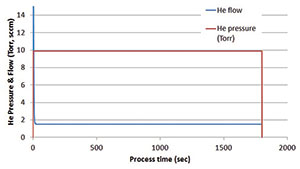
Figure 1. Good heat transfer is possible with electrostatic clamping, thanks to helium between the wafer and the electrode. Note that the helium backside pressure is constant, and the helium leakage is low and constant.

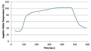
Figure 2. Maintaining wafer temperatures during aggressive plasma processing well below 140 0C prevents burning of the photo-resist
Moving to 150 mm
Like other sectors with the semiconductor industry, makers of LEDs are moving to larger wafers to cut costs. Benefits of making this move include increased yield, increased automation, and reduced wafer "˜touch time' "“ many of the same gains that drove the silicon industry to adopt larger and larger wafers.
However, it would be wrong to suggest that all LED makers are making the transition to 150 mm sapphire. Although leading LED maker Lumileds, for example, has been producing devices on 150 mm lines for several years − and is enjoying order-of-magnitude improvements in both LED die capacity and process yield by moving from 3-inch to 150 mm substrates "“ quite a few LED manufacturers have no plans to move beyond 100 mm in the foreseeable future.
The size of the wafers that are being used by LED makers governs whether it makes sense to perform batch or single-wafer processing of sapphire. The aggressive etch process needed to etch sapphire dictates that every wafer must have cooling, and performing this on a large batch makes sense for 2-inch, 3-inch and 100 mm wafers. However, this argument doesn't hold for 150 mm sapphire, which is falling in price, and in this case a single-wafer platform may be the best way forward for some, but not all, manufacturers.
Those LED chipmakers that are using 150 mm sapphire will hope to benefit from the plasma etch tools previously developed for mainstream silicon. However, the bad news for them is that such tools are not immediately suitable for etching sapphire. Dry etching is a very aggressive process, with much energy required to break sapphire bonds and remove material, and this can lead to heating of the wafer and the photoresist mask. Heat the mask above 140°C and it is destroyed.
To prevent overheating, wafers can be clamped to a temperature-controlled electrode. However, due to the low pressure in the chamber "“ it is less than 10 mTorr "“ there is a very limited heat conduction path between wafer and etch electrode. Adding helium gas, an approach often referred to as helium backside cooling, fills the void between the wafer and the electrode, leading to an improved conduction path. However, there is a penalty to pay for this: A pressure behind the wafer of several millibar, which will cause it to move if it is not clamped down.
One option for keeping the wafer in the right place is to mechanically clamp it, but this occurs at the expense of masking the wafer edge, and it may lead to particle generation. Due to these downsides, electrostatic clamping is more appealing − this is standard for silicon, but, unfortunately, it does not work well for highly insulating substrates. That's because sapphire electrostatic clamping relies on creating polarisation charges in the wafer, "˜stretching' the molecules to create dipoles, rather than displacing mobile charges. Consequently, there are several weaknesses associated with electrostatic clamping: the forces are much lower at the same clamp voltage; higher clamp voltages can cause premature failures in the electrostatic clamp table itself; if the table is robust enough, higher voltages can lead to polarisation of the dielectric layer of the electrostatic clamping itself, and then clamping is lost; and polarisation charges can take more time to create and to dissipate than mobile charges in a semiconductor, so it can be more challenging with sapphire to set up clamping and achieve reliable de-clamping.

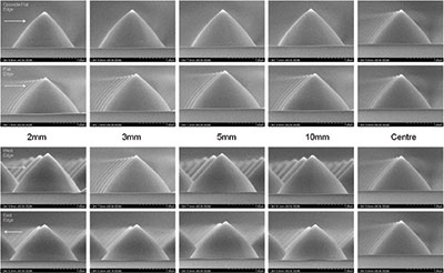
Figure 3. The PlasmaPro100 Polaris is capable of maintaining the profile of the features very close to the edge of the sapphire wafers.
At Oxford Instruments Plasma Technology in Yatton, UK, we have overcome these issues by developing a proprietary technique that allows electrostatic clamping of bare sapphire. This patent-pending approach (the inventors on the application are Y Song, J Ferreira and M Cooke) is capable of gripping 150 mm sapphire, even during the cooling process (see Figure 1 for results demonstrating constant clamping of a bare sapphire wafer for thirty minutes during etching).
With electrostatic clamping, some helium will always flow from out of the back of the wafer. Our measurements taken during the development of our clamping process reveal that this flow of helium is stable and relatively low, which is indicative of a constant clamping force. Efficient heat removal from the sapphire is then possible, while maintaining a constant backside helium pressure. Readings of wafer temperature show that this never gets close to 140°C, the temperature at which the photo-resist can burn (see Figure 2).
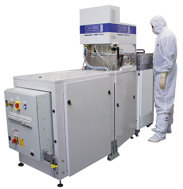
Preventing damage to the photoresist has enabled us to develop and launch the PlasmaPro100 Polaris, a single wafer tool with electrostatic clamping that is capable of etch rates above 100 nm per minute. When a wafer is loaded into this tool it is clamped and cooled, before a BCl3 plasma is created within the process chamber.
Each gripped sapphire wafer is attached to an electrode, and applying RF power to this leads to the acceleration of ions generated by the plasma. These charged particles bombard the wafer, removing both sapphire and photoresist. Where photoresist remains, the area under the pattern is not etched.
However, the nature of this process and the photoresist shape means that the footprint gets smaller and smaller as the action progresses, leading to sloped features that are transferred to the surface of the sapphire wafer.
The process is completed when all of the photoresist has been removed. At this point, there are domed or pointed features across the wafer.
Optimising the dimensions of these features enables the production of LEDs with superior performance. One current trend within the LED industry is to move to higher features with a very flat sidewall, and to form cones rather than domes. In this regard, dry etching offers a key advantage over a wet etch, because the final pattern can be selected by making adjustments to the photoresist mask. With this etching technique it is possible to produce a sapphire surface with a vast array of high, sharp cones that hold the key to GaN films with a lower defect density and LEDs with increased light extraction.
To trim manufacturing costs, chipmakers use as much of the wafer as possible to produce LEDs. With our electrostatic clamping, yields can be incredibly high, because the profile shape of the features is maintained to within 2 mm of the edge of the wafer (results shown in Figure 3 were obtained with an etch rate of 150 nm per minute and a selectivity to the photoresist mask in excess of 0.7:1).
This capability will help to bring down the cost-per-LED of producing patterned sapphire. What's more, as our tool can also enable optimisation of the shape of the etched features "“ leading to improved film quality and increased light extraction "“ it will be able to play a key role in bringing cheaper, brighter LEDs to market.


