
Delivering tomorrow
Can a new US-Ireland collaboration break down the materials barriers to next-generation GaN-on-silicon power electronics devices, asks Compound Semiconductor.
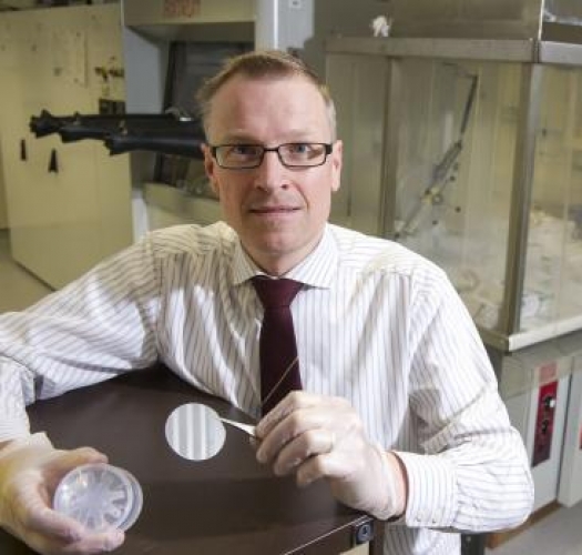
Peter Parbrook from Tyndall National Institute is to lead 'GaNnano', a project to develop GaN nanorod vertical devices. [Tyndall]
It's early days yet, but a new US-Ireland project that is exploring the best way to build GaN nanorod vertical device architectures is set to have a real impact on the global electronics industry.
As developers of heteroepitaxial structures strive to relieve the strains that kill performance in GaN-on-silicon diodes and transistors, research and development into defect-free nanostructures is gathering momentum.
Be it nanowires, nanorods and even nanopyramids, researchers worldwide are devising myriad methods to grow arrays of GaN nanostructures onto buffered silicon substrates.
These relatively strain-free structures contain fewer of the dislocations that cause leakage currents, and are set to form the basis of better performing high voltage power devices.
But demonstrating a cost-effective, high performing device on a silicon wafer is proving difficult, which is where the €1m Nano-GaN Power Electronics Devices - GaNnano - project comes in.
Comprising researchers from the Tyndall National Institute, Queens University Belfast and the Illinois Institute of Technology, the project aims to get to grips with the defect mechanisms that lead to leakage currents and electrical breakdown in these next-generation devices.
As project leader Peter Parbrook, from Tyndall puts it: "Can we get rid of the dislocations, to get rid of the breakdown routes, without having to go to the expense of buying expensive GaN substrates?"
The researchers will kick-off the project by growing nanorod arrays on sapphire substrates - with a view to investigating defects in these structures - and then move onto silicon wafers.
Parbrook is reluctant to reveal details on his nanorod growth methods but confirms growth will take place via MOCVD, with a patterned selective growth mask used to control the location, orientation of the nanorods, a few hundred nanometres in diameter.
He also points out how his team will be doping the GaN nanorods with silicon, used in the past to boost charge concentration and mobility within the structures. "When you dope GaN with silicon, the dislocation behaviour [within the material] changes, so we will also look at how this alters dislocation movement within the rods," he explains.
But crucially, the researchers will be focusing on the properties of nanorods arrays, rather than individual structures. "A lot of LED research has been based on getting results with an individual rod," says Parbrook. "But extrapolating from here to something you can manufacture is not a trivial exercise. We're looking at arrays and there's a lot of interesting science in this."
 SEM Image of nanostructured GaN formed as part of the preliminary study for this programme.
Materials characterisation of these structures will take place at Queens University Belfast, as part of a team led by Miryam Arredondo-Arechavala, with an emphasis on exploring dislocation formation mechanisms.
"Researchers here will be using scanning electron microscopy to see, [for example], if the defects bend out of the rods, or if we can grow them out of the rods," says Parbrook.
"Many researchers also say nanorods are dislocation free as the structure is so small it is no longer energetically favourable for the dislocation to form within the rod," he adds. "We intend to look at more nanorods than you would normally, to see if this really is the case."
At the same time, researchers will scrutinise material uniformity across arrays. "If we see defects in, say, every 54th nanorod and we're trying to make 100 then we have a problem," says Parbrook. "There are a lot of issues that still need to be solved."
But GaNnano is not all about materials characterisation. At some point throughout the three year-long project, Parbrook and colleagues intend to demonstrate the potential for, if not build, a GaN nanorod-based vertical transfer device, at the very least a Schottky diode.
To this end, the researchers are working with John Shen from Electrical and Computer Engineering at the Illinois Institute of Technology who, with his students, will simulate, model and test potential devices.
As Parbrook highlights, the first target will be to prove Schottky diodes actually work, but Shen has also proposed other novel device structures.
"Shen has a whole pile of different geometries we could eventually look at, and importantly is also very plumbed in with industrial partners," says the researcher. "He provides the device focus that industrial partners will want to see."
So after the project's three years, what might Parbrook like to see next? Clearly fabricating structures on silicon substrates makes six inch wafer sizes a must, and the researcher concurs.
"Ultimately we want a process that is compatible with a six inch line to use amortized factories, and of course you want the benefits of scaling," he says. "And devices will be 600V plus, eventually we want to be in that game."


