
LEDs: a potent package
In the race to cut LED manufacturing costs, Plessey, UK, unveils bold plans for bigger wafers, chip-scale packaging and more.
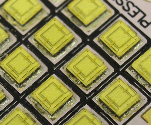
GaN-on-silicon LEDs: Plessey's plans for chip-scale packaging are underway.
As the LED lighting revolution shines on, industry players are now focusing on cutting manufacturing costs to drive LEDs further into the general lighting market. Today, GaN-on sapphire is the mainstream technology for LED manufacturing but industry interest in GaN-on-silicon is rising.
Clearly the cheaper silicon substrate holds appeal, but the opportunity to manufacture on amortized six inch and eight inch CMOS lines is where the real interest lies, a fact that hasn't been lost on LED manufacturer, Plessey.
The UK's leading LED light has been fabricating GaN-on-silicon LEDs on six inch wafers from its Plymouth plant - originally a six inch CMOS line - for at least two years, and is now looking at the next step.
"Our programme of work on eight inch substrates starts next month," says Keith Strickland, chief technology officer from Plessey. "There's no significant technical hurdles to overcome, it's more a case of when you take the commercial decision to do this."
"Some equipment in the line will eventually need to be converted from six to eight inch, and we could start to see that taking place in the next eighteen months," he adds.
But the future for Plessey is about so much more than wafer size. Intent on cutting GaN-on-silicon costs, the company now plans to ditch the traditional plastic GaN-on-sapphire tailored LED packaging and instead move towards cheaper silicon-based advanced packaging technology.
Today, the vast majority of LEDs are sold in plastic packages developed for GaN-on-sapphire LEDs. These predominantly lateral devices emit light in all directions, including through the transparent sapphire substrate, so packaging is sculpted on the inside to reflect as much light back out of the package as possible.
But as Strickland highlights: "GaN-on-silicon LEDs are surface emitters so if we put our device inside a plastic package designed for a sapphire device, it's doing nothing for us at all, and indeed can have a detrimental effect on light output efficiency."
 Plessey's Keith Strickland: "We will produce a chip-scale package with multiple components this year".
So, chip-scale packaging is the first step, and Plessey has already produced packaged LEDs that partners are currently sampling. Here, the GaN-on-silicon LED is mounted directly onto a silicon sub-mount, which of course thermally matches the GaN on Silicon LED, and crucially, the final packaged LED is much smaller than its plastic-packaged counterpart.
"Our perspective on this, is that the IC industry moved to chip-scale packaging a long time ago and a lot of technology is already in place for this," explains Strickland. "We can take advantage of this, so will now move to chip-scale packaging for our LEDs."
But the packaging developments don't stop here. The next step is to integrate multiple die into a package to produce high density LED arrays for applications from automotive headlamps to intelligent LED displays.
"We will produce a chip-scale package with multiple components this year and then within the next two years integrate more systems into the packaging," says Strickland. "We may start seeing early prototypes next year; this is largely driven by the partners we are working with."
Driving costs down
Akin to the IC industry, even cheaper wafer-level packaging comes next with Plessey also planning to ditch traditional wire bonds and use high performance, high density through-silicon via interconnects at the LED device level.
And finally, the company intends to integrate more functionality onto the chip, say photodiodes and FETs, to develop intelligent LEDs. Dubbed application specific LEDs, these devices will target on-chip diagnostics and sensors, as well as connectivity and communications applications.
"We have a direct analogy with the IC industry here," says Strickland. "In the early days you had many discrete components, then these were pulled together to deliver more monolithic solutions. This is where we see GaN-on-silicon LEDs have a real play in the lighting market."
"We are now working with partners that are close to the end applications, so we can understand what the problems are we actually solving here; this has to be commercially viable," he adds.
But intelligent LED vision aside, operations at Plessey, UK, continue as planned. Strickland confirms manufacturing will remain firmly in place in Plymouth with prototype packaging having been brought into the plant to help speed development. "Ultimately, we'll be looking at Application Specific LEDs here as well," he says.
Two MOCVD reactors are in place at the plant with orders underway for two more, edging towards the eventual aim of having many more reactors to produce 1.5 billion mm2 of LEDs per year. And the company has its eyes on more than LEDs.
"GaN-on-silicon also has an important play into power markets, so industry may see some transition here," concludes Strickland. "There is reasonable evidence to suggest that this market could eventually be bigger than the LED market, and we are already looking at this at a research and development level."


