
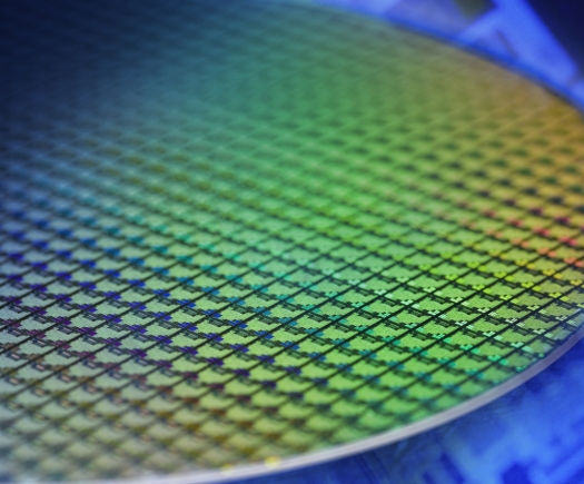
Imec presents technologies for advanced logic scaling
At this week's VLSI 2015 Symposium in Kyoto (Japan), Imec reported new results on nanowire FETs and quantum-well FinFETs towards post-FinFET multi-gate device solutions.
The research into advanced logic scaling is performed in cooperation with Imec's key partners in its core CMOS programs including Globalfoundries, Intel, Micron, Panasonic, Samsung, SK hynix, Sony and TSMC.
As the major portion of the industry adopts FinFETs as the workhorse transistor for 16nm and 14nm, researchers worldwide are looking into the limits of FinFETs and potential device solutions for the 7nm node and beyond. Two approaches, namely Gate-All-Around Nanowire (GAA NW) FETs, which offer significantly better short-channel electrostatics, and quantum-well FinFETs (with SiGe, Ge, or III-V channels), which achieve high carrier mobility, are promising options.
For the first time, Imec demonstrated the integration of these novel device architectures with state-of-the-art technology modules like Replacement-Metal-Gate High-k (RMG-HK) and Self (Spacer)-Aligned Double-Patterned (SADP) dense fin structures.
By building upon today's advanced FinFET technologies, the work shows how post-FinFET devices can emerge, highlighting both new opportunities as well as complexities to overcome.
Imec and its technology research partners demonstrated SiGe-channel devices with RMG-HK integration. Besides SiGe FinFET, a unique GAA SiGe nanowire channel formation during the gate replacement process has been demonstrated. The novel CMOS-compatible process converts fin channels to nanowires by sacrificial Si removal during the transistor gate formation.
The process may even enable future heterogeneous co-integration of fins and nanowires, as well as Si and SiGe channels. The work also demonstrates that such devices and their unique processing can lead to a twice or more improvement in reliability (NBTI) with respect to silicon FinFETs.
Moreover, Imec demonstrated Si GAA-NW FETs based on SOI with RMG-HK. The work compares junction-based and junction-less approaches and the role of gate work function for multi-Vt implementations. New insights into the improved reliability (PBTI) with junction-less nanowire devices have been gained.
Extending the heterogeneous channel integration beyond Si and SiGe, Imec demonstrated for the first time strained Ge QW FinFETs by a novel siliconi-fin replacement fin technique integrated with SADP process. Our results show that combining a disruptive approach like fin replacement with advanced modules like SADF-fin, RMG-HK, direct-contacts can enable superior QW FinFETs. The devices set the record for published strained Ge pMOS devices, outperforming by at least 40 percent in drive current at matched off-currents.


