Instant imaging with terahertz lasers
Wafer-bonding can create powerful terahertz lasers for real-time imaging of hidden weapons, illicit drugs and forms of cancer
BY MARTIN BRANDSTETTER, CHRISTOPH DEUTSCH, MICHAEL KRALL AND KARL UNTERRAINER FROM VIENNA UNIVERSITY OF TECHNOLOGY
One of the most appealing superpowers held by science fiction heroes is X-ray vision. By seeing through physical matter and revealing hidden objects, they uncover what is believed to be held secret and are able to foil the plans of villains.
Back in the real world, X-ray vision is also valued, because it can aid security checks and provide quality control. But it suffers from a massive drawback: Due to high photon energies, radiation at X-ray wavelengths is ionizing and exposure to it is harmful.
A possible alternative exists at the opposite end of the electromagnetic spectrum, towards the microwave region. In this spectral range, radiation is not ionizing, thanks to photon energies that are orders of magnitude below those of X-rays. What's more, microwaves can penetrate materials that are opaque in the visible, so it can reveal the contents within containers, which is why this technology is already being used in security scanners at airports. However, although this technology is convenient for imaging large objects, and people as a whole, its resolution is limited by the wavelength of the source "“ and that is of the order of a millimetre.
Fortunately, it is possible to find a spectral range that offers the best of both worlds "“ that is, one that avoids nasty blasts of ionizing radiation, while producing images that are sharp enough to uncover all the necessary details. Such attributes are found in the terahertz region that lies between the microwave and mid-infrared. Here radiation is non-ionizing, so is not harmful to biological tissue, and it has a wavelength of the order of 100mm, enabling adequate imaging resolution. Many materials have unique absorption characteristics in this spectral range, making this source of radiation ideal for accurate determination of different substances.
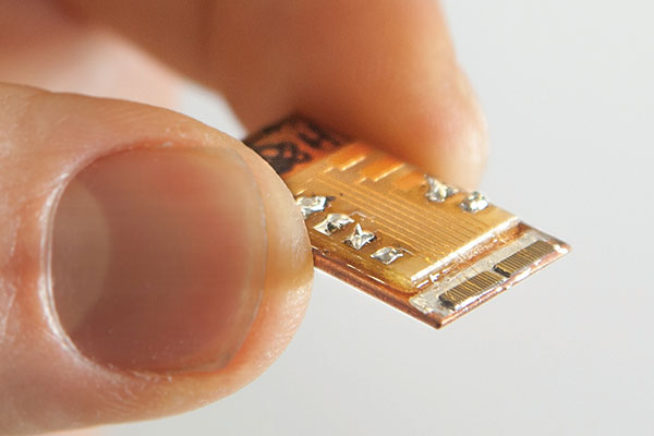
Thanks to these strengths, it is easy to think of many tasks that could be carried out with terahertz sources, including non-destructive material analysis, remote sensing and imaging. Such applications are not only interesting for scientific purposes − they also highly desirable for industry, biomedicine and security technology. And progress has already be made in this direction, with terahertz sources used today to detect cancers, identify illicit drugs and detect concealed weapons.
Holding back far greater deployment of terahertz imaging systems is the image acquisition time. Many techniques are based on a single detector element, which necessitates the scanning of an object. Depending on the desired resolution and the integration time, taking a single picture can take up to several minutes.
Fortunately, thanks to the rapid development of microbolometer cameras, recently it has become possible to perform real-time imaging. To do this, a high power terahertz source must illuminate the object. There are several ways to do this, but by far the most elegant is to use a quantum cascade laser (QCL) with sufficient power. Our team at the Photonics Institute at the Vienna University of Technology has developed such a source, which incorporates a wafer-bonded active region to increase output power.
Terahertz technologiesFor many years, the lack of any practical source of radiation has held back deployment of terahertz imaging (see Figure 1 for an overview of the sources). The options below 1 THz are dominated by: electronic sources such as resonant tunnelling diodes; semiconductor amplifiers that involve the use of multiplier chains; and vacuum techniques, such as backward-wave oscillators. In all cases, the source of radiation becomes very inefficient when approaching higher frequencies.
For frequencies between 1 and 5 THz, the selection of available sources is even more limited. Free electron lasers can emit huge terahertz powers, such as several kW, but they must be housed in large-scale facilities. Smaller options are the p-doped germanium laser, which can emit up to 10 W, but requires liquid helium cooling and a magnetic field "“ and the optically pumped terahertz laser, which can fit on a typical laser table. But every one of these classes of laser is impractical on account of its size, and this is hampering the large-scale implementation of terahertz imaging.
Far smaller and more convenient is the QCL. First demonstrated in 2002, this tiny III-V chip can span 1.2 THz to 5.2 THz and deliver powers exceeding 1 W. But even it is far from perfect: At present, it cannot run at room temperature, with the maximum operation temperature limited to about 200 K, making cryogenic cooling essential. If liquid helium or liquid nitrogen is used for cooling, a bulky source results, so a Stirling cooler is preferred, which is based on the compression and expansion of a gas, similar to a conventional refrigerator, and is able to achieve temperatures as low as 40 K. With this form of cooling, the terahertz QCL is still a very efficient source of radiation between 1 THz and 5 THz (see Figure 1).
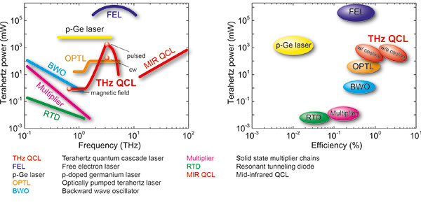
Figure 1. Comparison of available sources of high power terahertz radiation. The left panel shows the achievable terahertz power for different frequencies. The right panel compares the efficiency of the respective sources in the region between 1 THz and 5 THz by means of how much of the input energy is converted into terahertz radiation. Terahertz quantum cascade lasers are very convenient sources in this frequency region with respect to the output power and the efficiency, even if cryogenic cooling is taken into account.
Producing more power
To form QCLs, engineers must grow complex heterostructures featuring multiple coupled quantum wells that provide electron confinement in one direction. This form of bandgap engineering defines discrete energy levels − which translates into laser levels required for targeting a particular wavelength − and it governs carrier transport through the device. However, the active region is not the only major factor influencing the key characteristics of the laser, such as the output power, threshold current and maximum operation temperature. They are also dictated by the choice of waveguide. One common option, derived from microwave technology, is a microstrip waveguide (this may also be referred to as a parallel plate waveguide). Light is confined between a double-metal waveguide with sub-wavelength dimensions "“ it has a height of about 10 µm, while the emission wavelength is about ten times this.
This geometry has some pros and cons. The good news is that the facet reflectivity is very high due to the non-terminated microstrip line, thus the outcoupling losses are very low, allowing a high maximum operation temperature. But the downside is that the highly diffractive nature of the sub-wavelength aperture results in a poor far-field emission profile. To overcome this, the laser facet can be coupled to an antenna or to an optical lens (see Figure 2), enabling a ten-fold hike in extracted output power to more than 100 mW. Note that alternatives also exist for increasing the light extraction of double-metal waveguides, such as incorporating photonic crystals, metamaterials or distributed feedback structures into the laser.
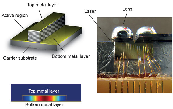
Figure 2. Illustration of a double-metal waveguide and the corresponding mode profile in the cross-section. The mode is squeezed into a sub-wavelength geometry, leading to an inefficient extraction of the optical power and a strongly divergent far-field. To couple the light out of the cavity more efficiently, a lens can be mounted on the laser facet, as shown in the right picture.
Another popular way for confining the light within the QCL is to sandwich the active region between a metal and a highly doped semiconductor plasmon layer. This combination leaks light into the substrate because the plasmon layer is partially transparent to the optical mode. A lower facet reflectivity results, boosting light out of the cavity (see Figure 3). But there is a price to pay for this: Reduced temperature performance, resulting from the low confinement of the optical mode within the active region.
Confinement within a QCL that sports a plasmon layer can be improved by simply increasing the height of the waveguide "“ a higher proportion of the laser mode is guided within the active region. Another benefit of this approach is the reduced interaction of the optical mode with the waveguide layers, thereby trimming the optical losses. And on top of these gains, more light is generated in the laser, thanks to an increase in the volume of the active region.
Turning to thicker waveguides is far from trivial, however. Heterostructures are grown by MBE, and the growth rates for this epitaxial technology are incompatible with thick structures.
An alternative approach, which we have pioneered, is to double the waveguide thickness by vertically stacking two individual active regions. This is accomplished with direct wafer bonding, a technique that avoids an interfacial adhesion layer. Instead, two semiconductor samples are literally fused together. This ensures excellent electrical and optical quality of the interface, and enables realisation of a successful device.
With our design, because one sample is bonded upside down on top of another, the active region must exhibit the same operation characteristics, in terms of threshold and gain spectrum, for both bias polarities (see Figure 4). To meet this requirement, we have developed a symmetric active region. In this structure, electron wavefunctions and thus operation characteristics are the same, regardless of the applied bias polarity (see Figure 5 for the bandstructure).
By stacking two active regions of this kind, pulsed output powers from a single facet have been propelled to almost 0.5 W. This is nearly four times the output of a device with single active region thickness. Our device is a very promising source for real time terahertz imaging. It could be paired with a focal plane array with individual pixel elements that are standard microbolometers, operated at room temperature. These elements are typically optimized for mid-infrared frequencies of around 10 µm, making them widely used for thermal imaging − but they are also sensitive to terahertz radiation, because the detection principle does not depend on the wavelength. This detector technology has come on in leaps and bounds in recent years, with device costs and system dimensions plummeting.
Another strength of our imaging system is that it does not require cooling with bulky cryogenic equipment. Instead, we use a compact Stirling cooler, which enables heat sink temperatures as low as 40 K. High thermal load powers of up to several Watts can be cooled, making this technique predestined for convenient operation of terahertz QCLs. We have constructed a compact imaging system using a microbolometer camera, terahertz optics and our QCL, which is mounted on a Stirling cooler and operated in a vacuum chamber. This delivers real-time
imaging (see the top panel of Figure 6, which depicts one frame of a recorded movie, which shows a razor blade partially covered in a security envelope).
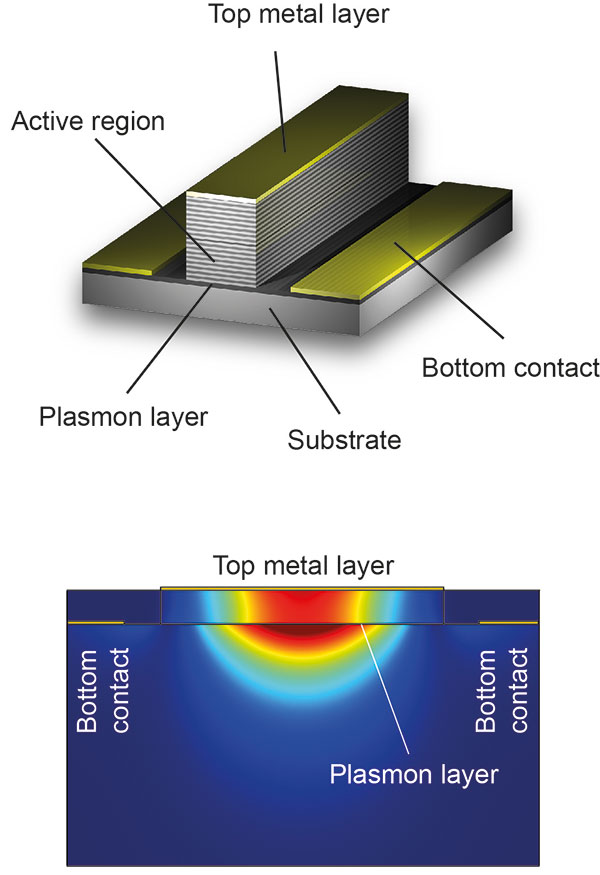
Figure 3. Illustration of a semi-insulating surface plasmon waveguide and the corresponding mode profile. The mode penetrates into the substrate and is thus not confined at a sub-wavelength scale, avoiding some disadvantages of double-metal waveguides.
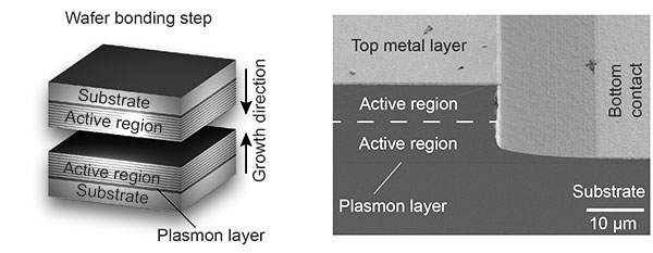
Figure 4. Illustration of the wafer bonding process. One active region is bonded upside down on top of the first one. Electrons are moving in the growth direction in one sample, and against it in the other one. Thus, the active regions need to operate the same way for both bias polarities. On the right, a scanning electron microscope picture of the cleaved laser facet of the device is shown.
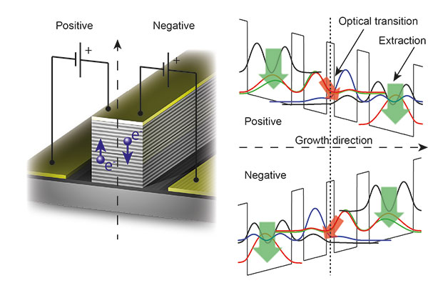
Figure 5. For the wafer bonding technique, a symmetric active region is necessary, showing the same characteristics in both bias polarities (positive or negative). The laser threshold and the gain spectrum are (almost) the same, regardless of whether the electron flow is in or against growth direction. The right picture illustrates the calculated bandstructure of a symmetric active region. The red arrows illustrate the lasing transition and the green ones the extraction transisiton from the lower laser level.
Demonstration of real-time terahertz imaging represents great progress, but in order for this technology to be widely deployed, there is the need for additional advances in the performance of the QCL. Managing the temperature of this device with a Stirling cooler is certainly a more practical approach than having to use liquid helium or nitrogen, but further improvement would result from a raising of the maximum operating temperature of the laser. If it could be extended to 240K, this would allow a switch to thermoelectric coolers, and ultimately a reduction in the dimensions of the imaging system.
Additional gains would result from more powerful QCLs. Such sources would aid real-time imaging and open the door to illuminating larger objects over greater distances. A great deal of effort is already being directed at this, with researchers in this field evaluating different active region designs, considering alternative material systems and developing improved waveguides.
There are also opportunities on the detector side, related to improvements in microbolometer cameras. These could be optimised for terahertz radiation. Gains have recently been made here, including the development of resonant antenna-like elements that drastically improve the signal-to-noise ratio and reduce the level of power required to illuminate an object. Although further progress is needed before terahertz imaging systems can be launched onto the consumer market, at least it is already possible to build versions today that are compact and convenient.
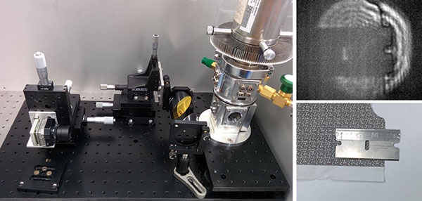
Figure 6. Real-time terahertz imaging setup. The right panel depicts one frame of a recorded movie, showing a razor blade covered by a security envelope (top). For illustration, a photograph of the blade outside the envelope is shown (bottom).


