GaN: The logical successor to silicon?
Stressor layers that crank up the speed of electrons are enabling a novel form of GaN-on-silicon transistor to offer a promising route to maintaining the march of Moore's law BY SUBRAMANIAM ARULKUMARAN AND GEOK ING NG FROM NANYANG TECHNOLOGICAL UNIVERSITY, SINGAPORE
50 years ago, writing in the trade magazine Electronics, a young engineer by the name of Gordon Moore predicted that with every passing year, the number of circuit components on an integrated chip would double. And history attests that not only was he right over the next decade, which was as far as he considered this projection to hold true "“ he was right through to today. This has meant that since 1965, when Moore penned his paper, the silicon industry has progressed from a chip by Fairchild featuring 64 components to Intel's Broadwell range of microprocessors that have a mind-boggling 1.3 billion transistors.
The driver behind this astronomical rise in the component count per chip has been the shrinking of the dimensions of the transistor. This allows more transistors to be packed onto a chip, and also leads to improvements in performance that are needed for practical reasons "“ for example, an acceptable power consumption for a transistor on a chip with 64 components is far less stringent than that on an IC sporting a billion transistors.
For many years, simply trimming the transistor's dimensions while maintaining its design wrought the kind of performance gains that were required for the next-generation of IC. But recently this has not been the case, so additional changes have been required, which have managed to prevent leakage currents from escalating. These steps include replacing the SiO2 gate with that made from HfO2 and switching from a planar device to that with a protruding fin.
The silicon industry is now preparing itself for its most radical change ever: the introduction of channels made from higher mobility materials. III-Vs are the leading candidates for electron transport, while germanium is being tipped to speed up the holes. Even the world's leading chipmaker, Intel, is arguing that new channel materials are needed, revealing at the International Solid-State Circuits Conference held February 2014 in San Francisco, that the limit for silicon is the 10 nm node. Beyond that there is a need to turn to high mobility materials to maintain the transistor's current while it operates at the lower voltages needed to ensure a decrease in the power that this device consumes.
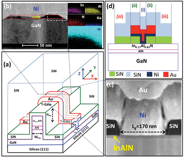
Figure 1 (a) The InAlN/GaN fin-HEMT is formed on a silicon substrate. (b) A cross-sectional, high-resolution transmission electron microscopy image (x-axis cut view) uncovers the different layers in the device, and electron dispersive X-ray analysis reveals the concentration of individual elements in a 176 nm fin. (c) A cross-sectional, high-resolution transmission electron microscopy image (y-axis cut view) of the device. (d) The T-shape gate has three different stress regions: the SiN/Au/Ni stress layers, the SiN/Au/Ni/SiN stress layers and the SiN/SiN stress layers.
Introducing III-Vs into the channel will not be easy, but some progress has already been made. At the European microelectronics research centre imec, engineers operating on a 300 mm silicon line have recently formed transistors with InGaAs channels that deliver an impressive level of performance. These developments are in line with the International Technology Roadmap for Semiconductors, which projects that the next generation of digital ICs will include high mobility finFETs that are formed on silicon wafers and feature channels made from III-Vs and germanium.
The researchers at imec, along with others working in this field, are investigating the ternary alloy InGaAs for high-mobility channels for the nFET. Results indicate that these devices are capable of operating at the lower voltages required for next-generation ICs, but the current delivered by them is not that encouraging.
One way to increase current by an order of magnitude, so it exceeds 4000 mA/mm, is to turn to a different type of transistor "“ a GaN HEMT. Formed on SiC substrates in a far larger form than that suitable for an IC, this type of device is already targeting high-frequency, high-power microwave and high-power switching applications, and by shrinking lateral and vertical dimensions, researchers have produced transistors with high currents that operate with an enhanced electron mobility. However, these transistors have several ailments, including a high gate leakage and a low ratio between the on and off currents. The upshot of these weaknesses is poor electrostatic gate control.
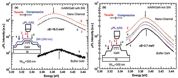
Figure 2. The position of the micro-photoluminescence peak produced by the InAlN/GaN nano-channel fin can uncover the stress within the structure. Spectra (a) with and (b) without SiN stress layer.
To address these weakness our team "“ made up of researchers from Nanyang Technological University, Singapore, Institute of Materials Research and Engineering, A*STAR (Agency of Science, Technology, and Research), Singapore and the The Ohio State University, USA "“ has developed lattice-matched InAlN/GaN HEMTs that feature a nano-channel fin structure. These are formed on silicon substrates, the only platform that is being considered for next-generation ICs.
One of the features of these devices is their intentionally introduced stress, realised through the incorporation of three different stressor layers in the nano-channel. These changes significantly enhance transport properties, even at a low operating voltage, which is one of the essential requirements for low-voltage logic circuits. The current in these devices is more than twice that in InGaAs FinFETs, while the electron velocity is more than 30 percent higher.
Formation of these transistors begins with the growth of a lattice-mtached InAlN/AlN/GaN device structure on a silicon substrate by MOCVD. We confirmed the composition with high-resolution scanning transmission electron microscopy and energy dispersive X-ray analysis (see Figure 1).
The key to the very high current density in our InAlN/GaN transistors has been the incorporation of three stressor layers that enhance the saturation velocity in the fin. The first, a 120-nm-thick layer of SiN, raps over the fins, while the second "“ the
Ni/Au T-gate "“ provides additional localized stress to this fin, due to a combination of metal in the foot-print, and the pairing of SiN and metal at the head. A PECVD-grown, 120 nm-thick passivation layer of SiN that covers the entire structure provides the third contribution to stress.
According to micro-photoluminescence spectroscopy, the in-plane tensile stress that results from the triple stressor is 0.47±0.02 GPa (see Figure 2). A similar figure has been obtained by micro-Raman spectroscopy, a technique that suggests a tensile stress of 0.39±0.12 GPa (see Figure 3).
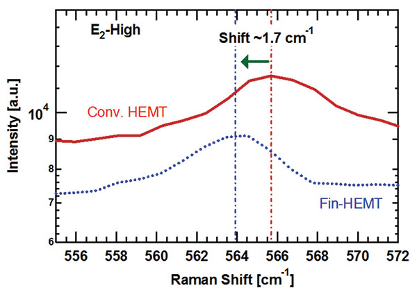
Figure 3. Micro-Raman spectrum (E2-High) of a InAlN/GaN nano-channel fin without a SiN stress layer.
Electrical measurements on our novel fin-HEMTs verify the benefits of stress. At a drain-source voltage of 6 V, the maximum drain current is 3940 mA/mm, while the transconductance is a record breaking 1417 mS/mm (see Figure 4). Using a two-dimensional model, it is possible to extract an electron velocity of 6.0à—107 cm/s, which is nearly 90 percent higher than that of the conventional In0.17Al0.83N/GaN HEMT (see Figure 5). We believe that this record-breaking velocity stems from variable stress along the nano-channel, which produces significant variations in the conduction-band-edge. Such variations could create an electron launcher effect, leading to a quasi-ballistic transport across the channel, and thus resulting in a hike in electron velocity.
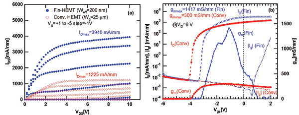
Figure 4. (a) Current-voltage (b) and transfer characteristics of conventional InAlN/GaN HEMTs and three-dimensional triple T-gate InAlN/GaN nano-channel fin-HEMTs.
There is good reason to believe that our devices have excellent high-frequency characteristics. Our measurements on a conventional InAlN/GaN HEMT reveal a cut-off frequency (fT) of 70 GHz, a value that agrees with that from a simple equation linking electron velocity to effective gate length. In comparison, our nano-channel device exhibits a record-breaking fT of 560 GHz, after plugging in the record-breaking transconductance to a related equation. This is the highest fT for any GaN-based HEMT.
It would be good to back up these extracted values with direct measurements of fT. However, that's not easy. It is tricky to determine the fT values using S-parameter measurements, due to the existence of large device parasitics.
The transistors formed on SiC using AlGaN/GaN technology are better than our devices in one regard, having a superior maximum drain current "“ it can be in excess of 4000 mA/mm. However, the transconductance for these rivals is only around 1000 mS/mm at a drain-source voltage of 3 V. What's more, fabrication of such a high-performance device requires some very complicated processes, such as the formation of deep gates with dimensions below 20 nm, self-alignment processes that use a source-drain gap of 100 nm, and an expensive re-growth technology to suppress parasitic resistances. And compounding all of these issues, these conventional devices are hampered by short-channel effects.
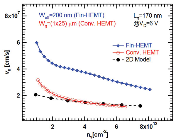
Figure 5. Extracted electron velocity for three dimensional triple T-gate InAlN/GaN nano-channel fin-HEMTs.
In sharp contrast, our proposed device is easier to make, while having the capability to deliver record performance. It can be fabricated using conventional electron-beam-lithography or stepper technologies, approaches that can form nano-channels and conventional sub-micron T-gates. What's more, our devices are not produced by encroaching on the limit of what is possible, but employ T-shaped gates of 170 nm "“ far larger than the 70 nm to 80-nm I-shape gates on 88-nm fins used by other research groups.
One implication of this situation is that we should be able to deliver an increase in performance through a reduction in device dimensions, such as a smaller fin width and gate-length. To do this we will need to optimise the device layout and fine-tune the stress in the transistors with materials that have different dielectric constants.
Our device also delivers impressive performance at an operating voltage of 0.5 V, which is within the regime that will be used in next-generation microprocessors. At this voltage, the drive current is 1030 mA/mm, transconductance is 646 mS/mm, and the ratio of the on-current to the off-current is around 106. Compared to a conventional InAlN/GaN HEMT operating at the same voltage, our novel device has the upper-hand in many key areas, with the exception of transconductance (see Figure 6 and table 1). This weakness might be addressed, however, through scaling of the gate-length.
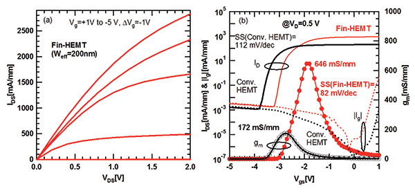
Figure 6. (a) Currentvoltage characteristics of a three-dimensional, triple T-gate InAlN/GaN nano-channel fin-HEMT. (b) A comparison of the electrical characteristics of an InAlN/GaN fin-HEMT and a conventional HEMT at an operating voltage of 0.5 V. Note that the measured Q-factor (gm/SS) of the fin-HEMT is 7.9.
The extracted electron velocity in our nano-channel transistor is 2.6 x 107 cm/s, indicating an fT of 245 GHz, and implying that our device is capable of high-speed operation at the low operating voltages that will be employed in tomorrow's microprocessors. But before it is deployed there, we will need to develop an off-state device "“ so far, all we have made is a D-mode, normally on device.
To do this, we can use E/D (normally off/normally on) type logic switches. It is possible to make an E-mode fin-HEMT by trimming the width of the fin, indicating that it should be easy to integrate E-mode (normally-off) fin-HEMTs with D-mode cousins on a single chip. This will allow us to demonstrate low driving voltage E/D logic circuits that are based on our stress-engineered transistors, and ultimately showcase a very promising route for maintaining the march of Moore's Law.
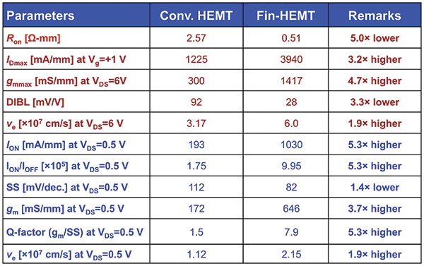
Table I. Benchmarking of InAlN/GaN nanochannel fin-HEMTs with conventional InAlN/GaN HEMTs


