
Plessey eyes eight inch wafers
Government cash will help UK LED manufacturer, Plessey, migrate more quickly to eight inch wafers. Compound Semiconductor finds out how.
A €1.3 million grant will drive Plessey closer to eight inch processes.
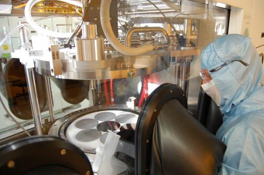
While Plessey Semiconductors is in the midst of fabricating GaN-on-silicon LEDs on six inch wafers at its UK-based Plymouth plant, a recent cash injection from UK government is set to speed up its transition to eight inch wafers.
In mid-July, the UK-based LED manufacturer won €1.3 million as part of the Advanced Manufacturing Supply Chain Initiative (AMSCI), to accelerate high volume manufacturing of its GaN-on-silicon LEDs in Plymouth.
Working with partners, Aixtron and Bruker Nano Surfaces, the company intends to increase the yield of its current GaN-on-silicon process while getting ready for eight inch commercial production.
"The grant will be used for a combination of buying new capital equipment, and research and development labour activity," says Plessey chief technology officer, Keith Strickland. "We're buying some measurement and metrology tools for the project and [spending] the rest on the labour and engineering associated with the use of those tools."
For starters, Plessey will invest in a Bruker LumiMap electroluminescence tool designed for optical and electrical characterisation on epiwafers for high brightness LEDs.
Key measurements include forward and reverse IV characteristics, spectral intensity, wavelength and spectral width measurements. And as Strickland puts it: "This takes away the need for wafer processing so we can speed up wafer characterisation, when the wafer comes out of the MOCVD tool."
As part of the grant, Plessey is also working closely with Aixtron, to address the necessary MOCVD reactor re-tooling issues of moving from six inch to eight inch wafers.
For example, the deposition equipment manufacturer will be designing and building new susceptors - the reactor plate that holds the substrates - so its MOCVD reactors can handle the larger wafer sizes.
"How the wafers fit into the susceptor pockets is very critical to MOCVD growth," highlights Strickland. "The design of this and other aspects of the reactor will help with yields."
According to the chief technology officer, beyond re-tooling, no real technical hurdles exist for the move to eight inch wafers, but the commercial timing has to be right.
"We have to re-tool our wafer processing [instrumentation] as well as our growth reactors so there are significant costs associated with this," he says. "When you reach certain volumes, then the economic case is made, but you can't just switch overnight, re-tooling takes time."
And while Strickland won't comment on exactly when Plessey will make the final move to eight inch production, he confirms the grant will reduce the time until the transition.
"This [conversion] is an ongoing process," he says. "We are still working with six inch wafers at the moment, but have started working on eight inch wafers, although the conversion won't be imminent, as in this year."
"But this grant is important as it will help us to migrate more quickly to eight inch wafers," he adds. "As the time approaches for migration, we will have done some of the engineering ahead of time, so this funding will certainly help us to knock months off commissioning."
Cutting costs
Shorter time-frames aside, Plessey is also looking forward to the significant cost-savings that will ensue. An eight inch wafer provides approximately 40% more area on which to grow devices.
Yet, as Strickland puts it: "The cost of sending that wafer down the production line to fabricate these devices is only a small increment more. You have to invest in new pieces of equipment but fabrication doesn't scale-up inordinately, so this is a big benefit."
And importantly for UK government, this fabrication of these cheaper LEDs is kept onshore.
Plessey's latest government grant follows an initial €7 million AMSCI grant, won two years ago with UK LED developer, Zeta Controls, to build an indigenous sustainable manufacturing chain for solid state lighting.
"It is very good that we still get this level of funding as our previous grant was also very useful in helping us to put our assembly line in place," he points out. "This type of government funding means we are not having to manufacture offshore, and can also maintain our expertise in areas that would also normally go offshore."


