Glorious GaN takes centre stage at CS International
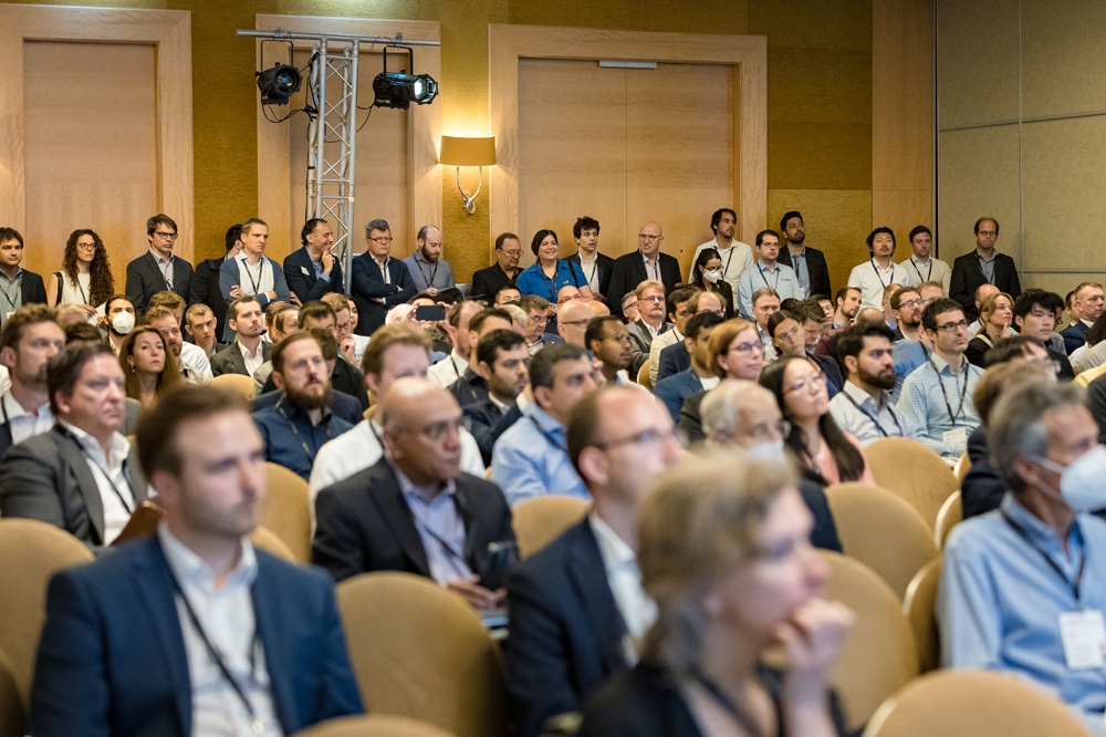
Speakers at CS International highlighted how GaN devices are now combining higher blocking voltages with exceptional efficiency, delivering incredibly high power densities in the RF, and covering all of the visible spectrum in the form of the microLED
Strengthening its well-established credentials, CS International continues to cover the biggest breakthroughs within the compound semiconductor industry.
At the most recent gathering of CS International, co-located with PIC International and Sensors International and held in Brussels on the 28-29 June 2022, leaders from industry and academia delivered almost 40 talks covering compound semiconductor devices and related materials. Those presentations were delivered in five sessions entitled: Fast, more fugal networks; Exploiting GaN’s glorious potential; Building a multi-billion dollar SiC industry; Superior surface-emitters; and Multiple markets for the microLED.
The 600 or more delegates at AngelTech, the umbrella name for CS International and its two co-located events, also benefitted from tremendous networking opportunities in the exhibition hall. In this area, just outside the auditoria, those attending could converse with speakers or ask about the latest advances in equipment and support services provided by the 70 sponsors.
During the presentations at CS International, many widely held views within industry came under scrutiny. Those in attendance would have left pondering whether silicon really is the best substrate for GaN power devices, whether MOCVD is the most suitable technique for growing them, and whether AlInGaP is going to play a role in displays based on the microLED.
The switch to sapphire
For many years, SiC has been by far the most widely adopted foundation for making GaN RF devices. That’s not the case for power devices – this substrate is too expensive, so silicon dominates. But what about sapphire, which underpins countless LEDs? Could this have a role to play outside the optoelectronic domain?
According to Transphorm’s CTO Geetak Gupta, sapphire is a great option for extending the breakdown voltage of GaN power devices. He argued that for 1.2 kV transistors, FETs formed from GaN-on-sapphire can deliver an efficiency as high as 99 percent. That’s enough to outperform SiC MOSFETs, and will enable GaN FETs to be in a strong position to serve in a new generation of electric vehicles, which will employ electronics with a breakdown voltage of around 1.2 kV in automobiles incorporating 800 V batteries – that’s double the standard battery voltage used today.
Note that Transphorm has no intention of switching the substrate of its 650 V GaN FETs from silicon to sapphire. That’s because these devices already have the upper hand over their SiC equivalents by offering an efficiency that’s 25 percent to 38 percent higher when delivering powers just short of 10 kW.
But at higher voltages the case for switching to sapphire is compelling. To produce a blocking voltage of 1.2 kV or more, the thickness of a GaN epilayer on silicon must exceed 10 microns. That adds cost, hampers throughout and threatens to distort the wafer.
Here sapphire is a great solution, championed Gupta. He explained that it is cheap, widely available in the 200 mm format, its insulating nature allows a reduction in the total epitaxial thickness for a given blocking voltage, and wafers can be run through a CMOS-compatible line. What’s more, packaging and dicing can draw on GaN LED infrastructure.
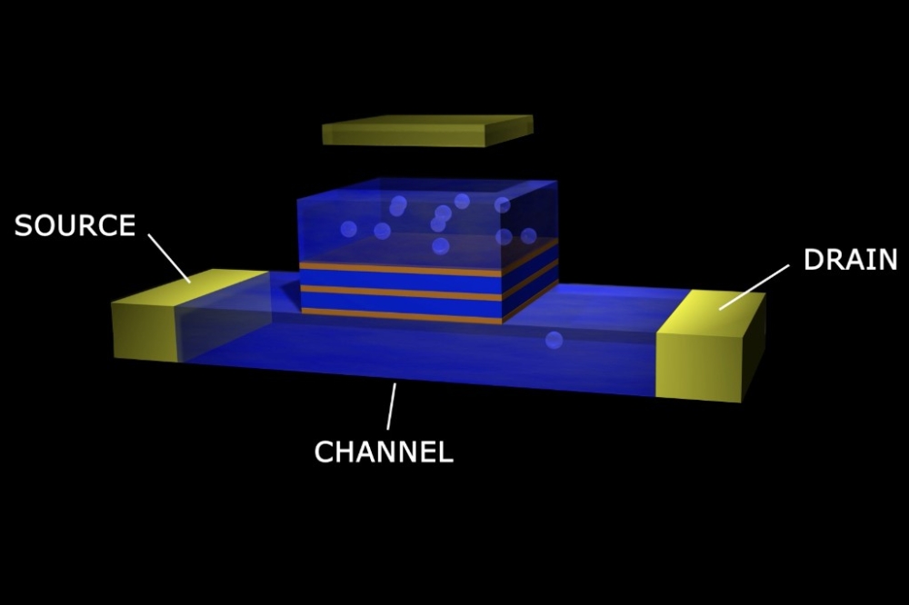
The team at Transphorm have produced a normally off device by combining a HEMT with a low-voltage silicon MOSFET. This hybrid, sporting a threshold voltage of more than 4 V and a leakage current exceeding 2 microamps at 1.4 kV (hard breakdown is 2 kV), can pass more than 160 A when driven in pulsed mode.
Sapphire’s weakness is its low thermal conductivity, but this can be addressed by thinning the substrate. Transphorm has reduced this to 200 micron.
Benchmarking the 1.2 kV FET with a buck-converter, which steps down the voltage from 900 V to 450 V at a 100 kHz switching frequency, showcases the potential of this GaN-on-sapphire technology. Conversion losses are 8-9 percent higher with a SiC MOSFET – and there is still room for optimisation of the GaN device, according to Gupta.
From MOCVD to HVPE
At CS International Kyma’s CEO, Heather Splawn, challenged the standard growth technique for making GaN transistors, advocating “HVPE for HVPE” – a catchy phrase that is short for the use of hydride vapour phase epitaxy for high-voltage power devices. Splawn argued that for higher blocking voltages, such as 1.7 kV, devices should be vertical. This requires thick layers, which are better to deposit by the “faster and cleaner” HVPE process. Growth needs to be on native GaN, which is pricey today, but costs should come down as volumes rise, according to Splawn.
Kyma has a very strong pedigree in developing HVPE reactors for the growth of GaN epilayers. It produced its first HVPE growth tool back in 1998, and is now offering its sixth-generation reactor, named Katharo. This tool can accommodate wafers with a diameter up to 200 mm, and form bulk layers with a low carbon density at a growth rate of up to 150 microns per hour.
One of the criticisms of the HVPE technique is that it is inferior to MOCVD for the growth of sharp interfaces. Splawn and her colleagues are addressing this by developing technologies for moving from a high growth rate to a lower one, and from n-type to p-type material.
RF: Upping the voltage
When it comes to RF GaN, one of the handles for increasing performance is to turn to a higher supply voltage. Increasing the voltage provides a proportional boost to both the gain and the power density of the device. In addition, there is a change in the load-line resistance, generally making it easier to ensure impedance matching. The upshot of turning to a higher supply voltage is that it opens the door to a higher system efficiency at a lower cost.
A group at Fraunhofer IAF is pursuing this, developing GaN devices operating at 100 V. At CS International team spokesman Sebastian Krause described the challenges of going to higher voltages and the progress to date.
Krause explained that shifting to a higher voltage increases the strength of the electric field, and in turn may lead to trapping of carriers, impaired reliability, a hike in leakage current and diminished current gain. While all these concerns can be combatted with the introduction of field plates, this may introduce an additional output capacitance, which is a greater impediment at higher voltages.
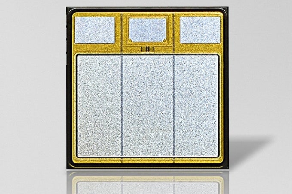
The team from IAF have used 4-inch SiC as the foundation for producing AlGaN/GaN HEMTs with a dual field plate and through-substrate vias. The resulting chips, each 1.5 mm by 3.75 mm, are capable of producing 600 W. “It’s not that big a device, especially when considering the power it produces,” remarked Krause.
RF measurements reveal a cut-off frequency of 10 GHz, suggesting the potential for operation through to the X-band. According to load-pull measurements at 7.2 GHz, power-added efficiency is 66 percent at 10 W/mm.
All across the visible
The production of full-colour LED-based displays involving direct emission tends to involve blue and green variants made with GaN an AlInGaP-based red emitters. A potentially simpler alternative is to just use GaN, but efficiencies plummet at longer wavelengths, due to material issues and strong internal electric fields.
However, it is still possible to produce GaN LEDs covering the entire visible range. Demonstrating this at CS International, Ellie Galanis from Porotech presented a video that showed a tiny pixel covering all wavelengths, as well as producing white emission. The workings of this microLED technology, referred to as Dynamic Pixel Technology, were kept under wraps, despite attempts from the audience to extract those crucial details. However, Galanis did reveal that changes in wavelength came from variations in the driving conditions of the pixel.
The core technology behind Porotech’s success is the generation of its porous GaN, which manipulates the strain threatening to thwart the efficiency of nitride LEDs in the red. Porotech has recently partnered with IQE to accelerate commercialisation of this approach.
Other materials
While GaN took centre-stage at this year’s CS International, there were plenty of talks detailing important advances with other materials. They included: Infineon’s expansion of SiC devices, occurring against a backdrop of a booming industry set to be worth $6 billion by the latter half of this decade (coverage of this session will be the focus of this year’s CS International conference report to be published in issue VI); Trumpf’s introduction of GaAs VCSELs with integrated optics (details are given in this feature from the latest edition VCSELs: Integrating backside optics; and NTTs development of InP membrane lasers to speed optical communication.
Further breakthroughs in a wide variety of compound semiconductor technologies are sure to sit at the very heart of next year’s CS International, which, following disruption from the Covid pandemic, will return to its traditional slot of early Spring. AngelTech is fixed for 18-19 April, located at The Sheraton Hotel in Brussels.


