News Article
Kyma announces key advances in its AlN and GaN on silicon (Si) template product lines
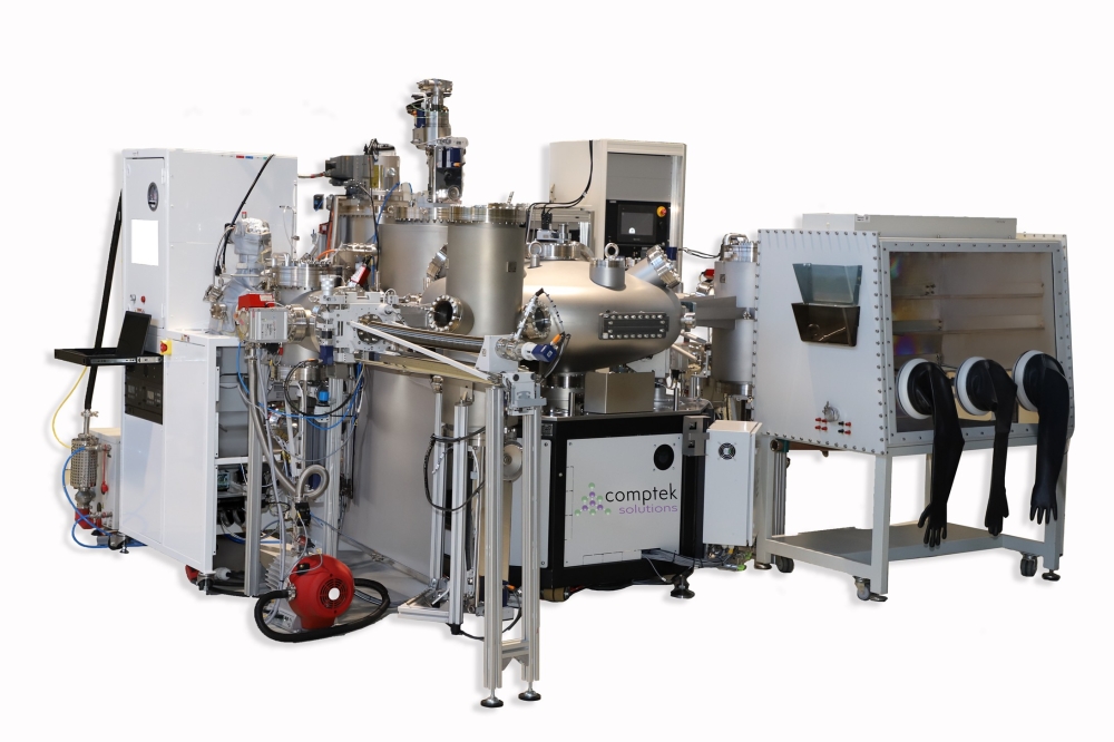
Kyma’s AlN on Si template products are fabricated using their patented plasma vapor deposition of nanocolumns (PVDNC) technology
Kyma’s AlN on Si template products are fabricated using their patented plasma vapor deposition of nanocolumns (PVDNC) technology, which provides an excellent surface for subsequent deposition GaN and AlN based device structures. Kyma’s GaN on Si template products are fabricated using their patented hydride vapor phase epitaxy (HVPE) technology which is performed on the PVDNC AlN on Si Template. The associated manufacturing processes are expressed as follows:
•PVDNC AlN Growth Process + Si Substrate = AlN on Si Template
•HVPE GaN Growth Process + AlN on Si Template = GaN on Si Template
Key improvements to and facts associated with Kyma’s AlN on Si Template process include the following:
•No slip lines
•Qualified for customer growth of semi-insulating GaN for FET applications
•AlN templates have been shipped in 2-inch, 100mm, & 150mm diameter form factors and has been demonstrated in 200mm and 300mm
Key improvements to and facts associated with Kyma’s GaN on Si Template process include the following:
•No slip lines
•Higher yield and more reliable process
•Faster and more reliable delivery schedules
•Available now in 2-inch and 100mm diameter
Kyma’s Technical Sales Engineer, Tamara Stephenson, stated “We are pleased to offer improved AlN and GaN on Si Template products and to shorten our delivery times too. Customer interest is great due to the device performance benefits that nitride semiconductor materials support, along with the cost and diameter advantages of an underlying silicon substrate.”
The market for nitride semiconductor devices was $9B in 2011 and is expected to reach $90B over the long term, including $60B in visible lighting applications and $30B in power electronics applications.
www.kymatech.com