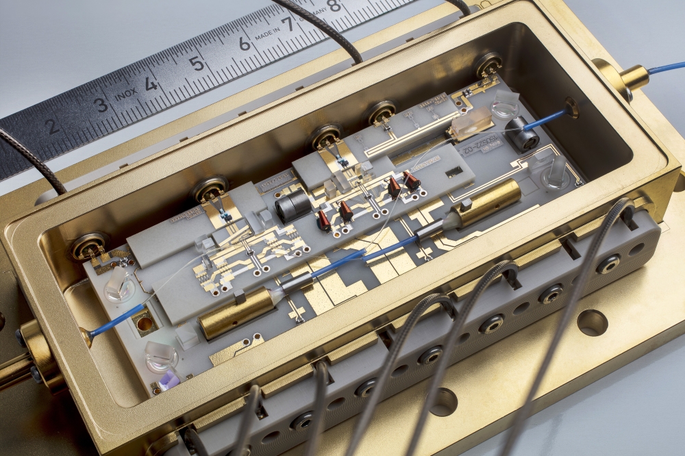
Toray develops high-speed III-V chip mounting technology
AI-driven demand for high-speed communications is fuelling the construction of more data centres, raising concerns about their heavy power demands. This has accelerated the development of both long-distance and short-range optical communications within data centres.
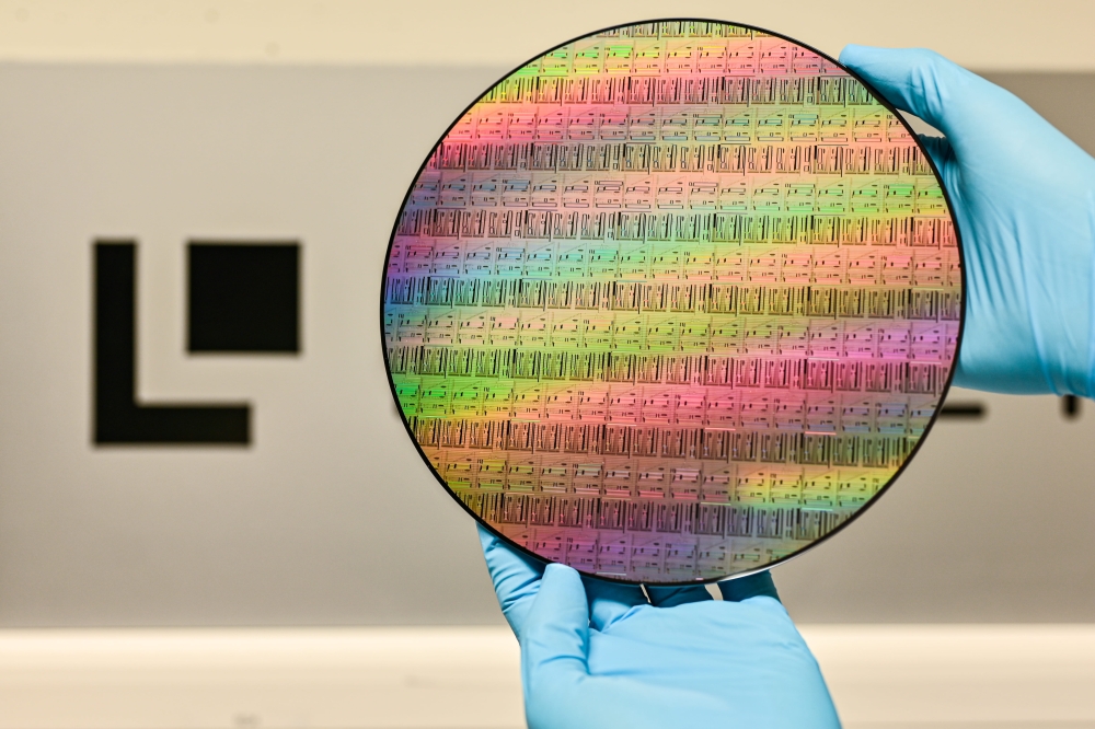
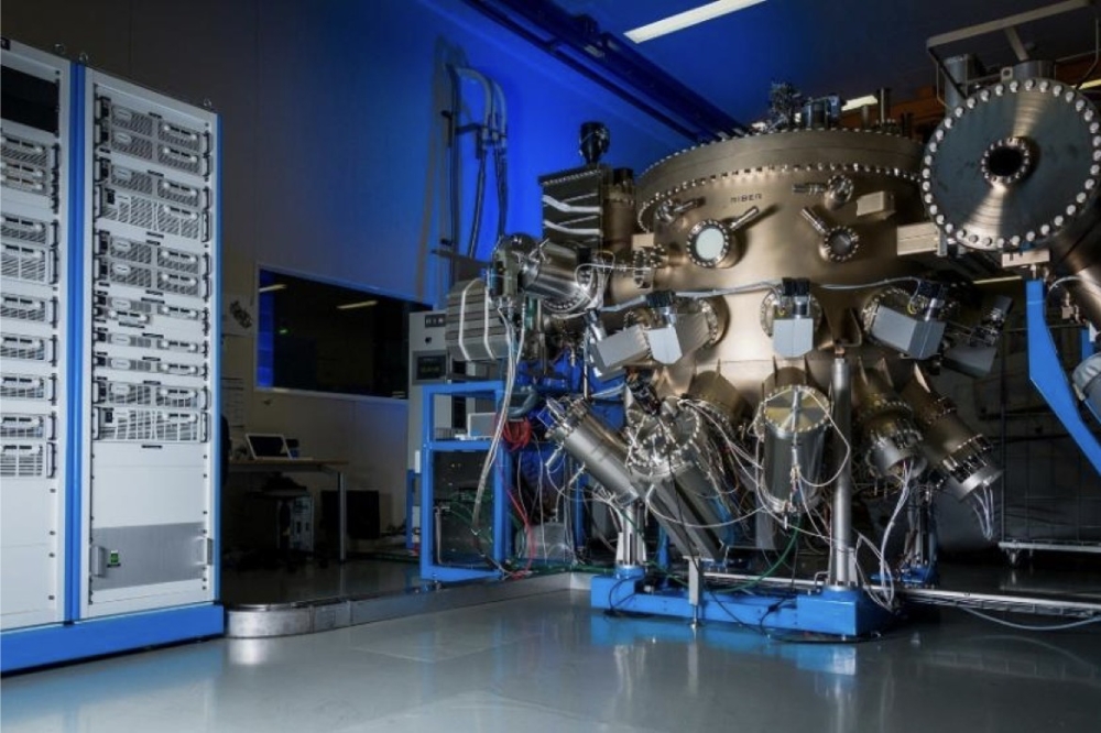
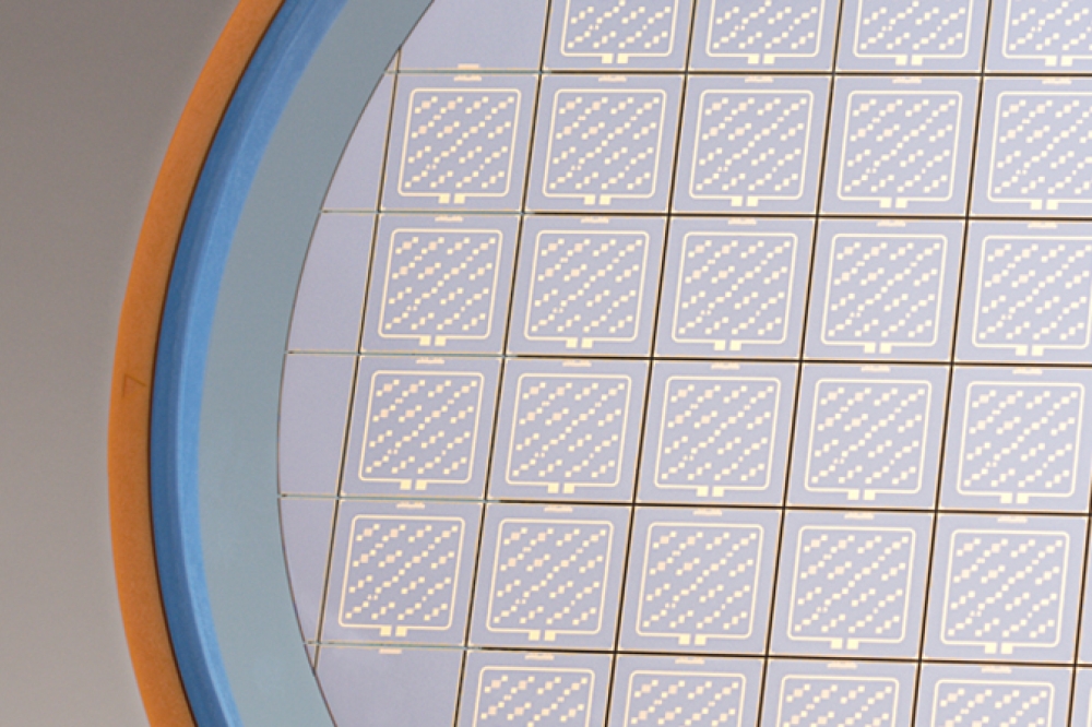
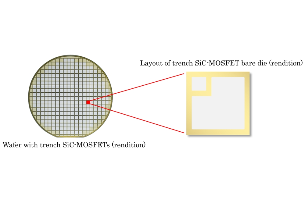
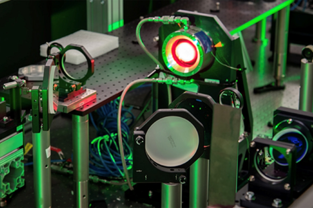
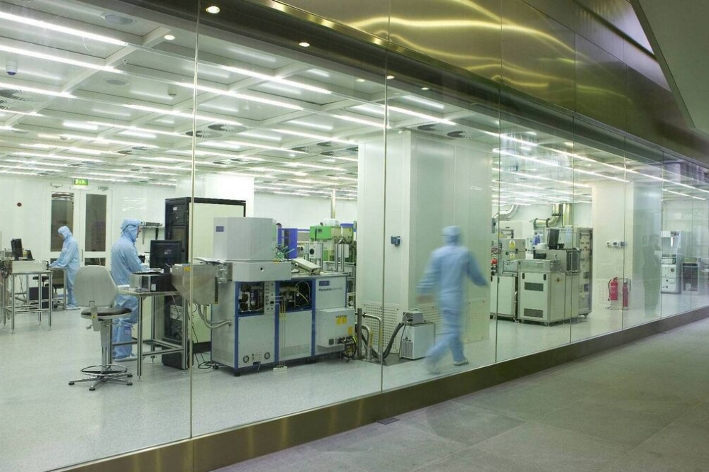
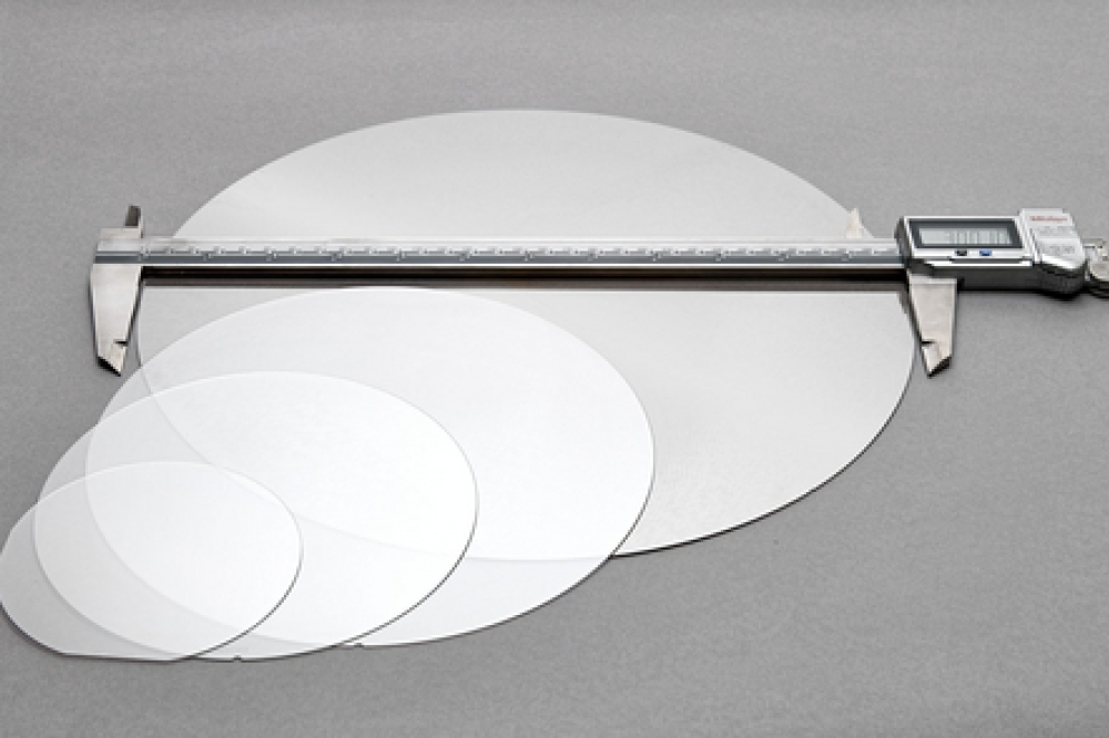
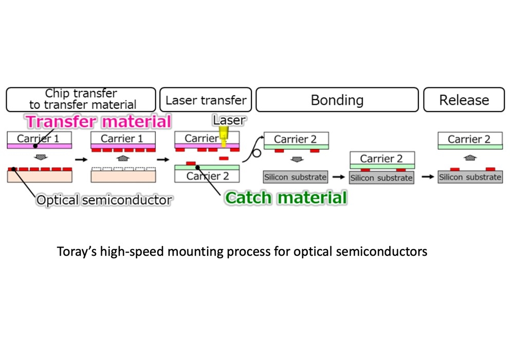
Along with the increasing use of silicon photonics has come the challenge of mounting optical semiconductors made from InP and other III-V compounds onto silicon. Mass transfer technology is essential to do this swiftly and in large quantities.
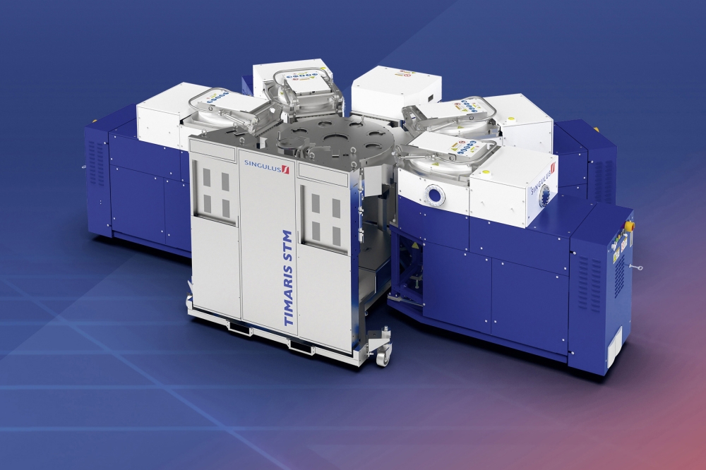
Toray, with subsidiary company Tory Engineering, has now developed a material for fast laser transfers of InP and other optical semiconductors. They have also worked on a material to 'catch' transferred chips and bond them directly to silicon substrates and a related mounting process technology.
They say these efforts have boosted optical semiconductor bonding speed to 6,000 units per minute,, compared with around four units per minute with conventional flip chip bonders.
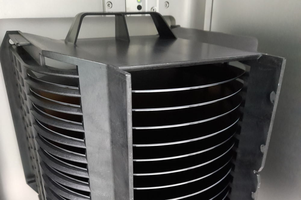
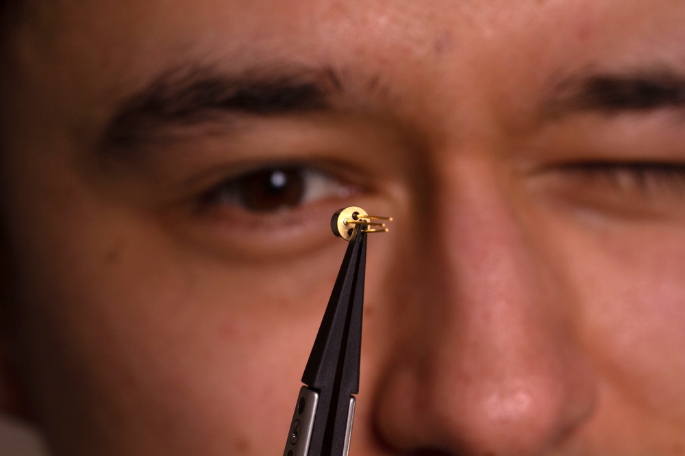
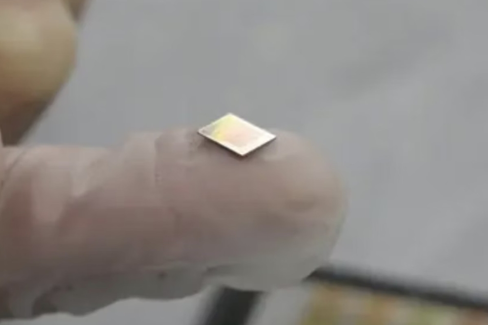
Toray previously developed transfer materials for micro LEDs. In this case, the InP-based optical semiconductors are 640 microns long and 90 microns wide and less than 3 microns thick. While longer and wider than general micro LEDs, the chips are also extremely thin. Toray developed a new material that enables transfer with a single laser irradiation without damaging chips, which should improve yields and throughput.
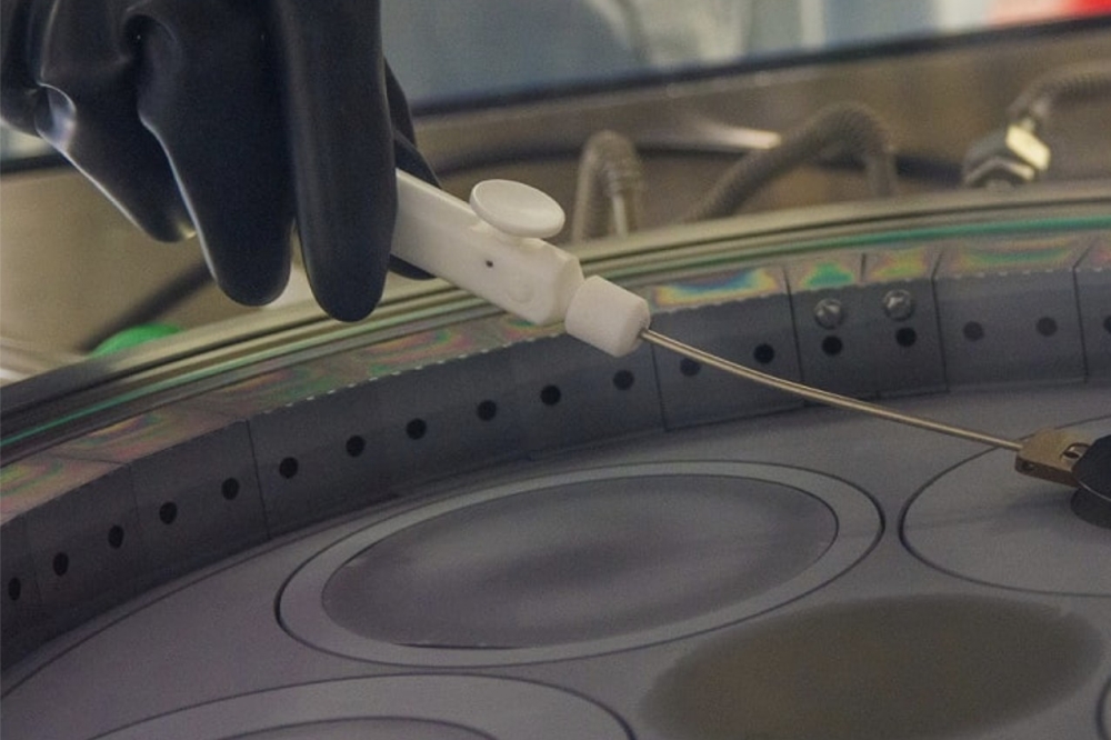
'Catch' material must not only capture fast-flying chips but also withstand the subsequent direct bonding of these chips to the silicon substrate after chemical cleaning and activating the bonding surface with plasma, pressurising under high temperatures of more than 200°C. Release must thereafter be easy. Toray says it employed years of expertise in designing heat-resistant polymers and controlling adhesive properties to develop a new catch material that makes this possible.
Toray has used these materials to collaborate with Toray Engineering in developing and demonstrating the entire process, from laser transfer to direct bonding on a silicon substrate. The company has confirmed that a post-bonding positional accuracy of ±2 microns and a rotational deviation of ±1°.
Toray says its next step is to verify chip operations and use actual devices to establish its technology. It will endeavor to enhance positional accuracy and broaden technology applications to include mass transfers of chips made from other different materials and millimeter-order semiconductor chips.
Toray developed part of this technology with a grant for the JPNP 20017 project of the New Energy and Industrial Technology Development Organization. This R&D initiative project aims to solidify the foundations of post-5G information and communications systems.