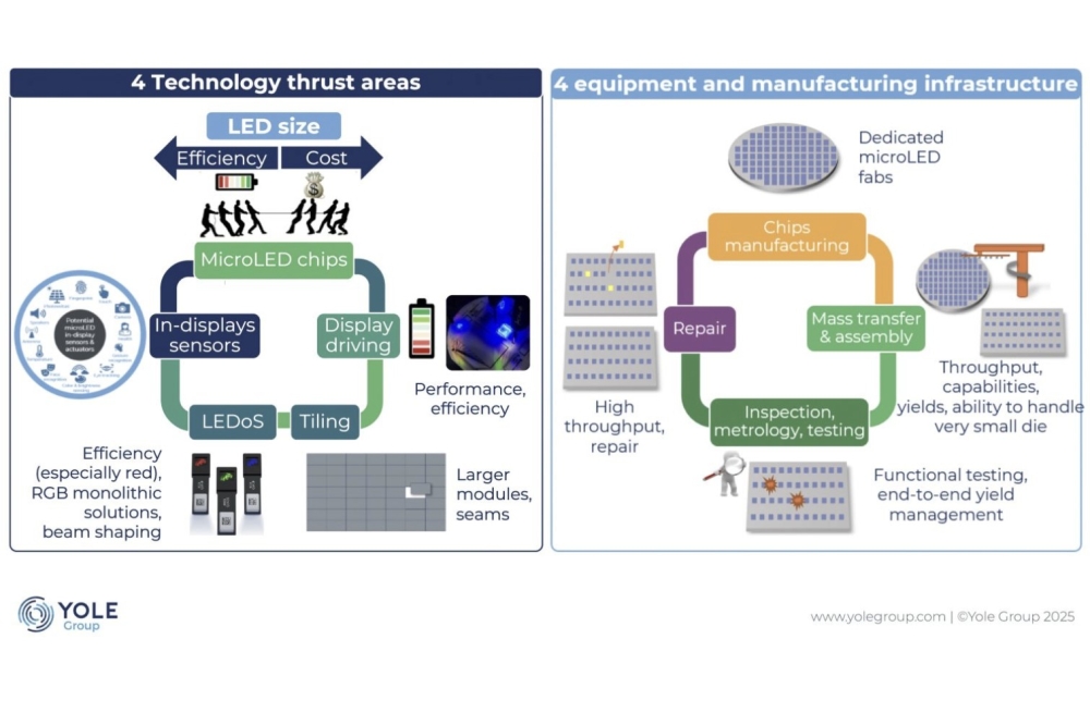
III-V labs celebrates 20 years
Focused on III-V R&D for its parent companies Thales, Nokia and CEA- Leti, III-V Lab is celebrating 20 years if successful innovation.
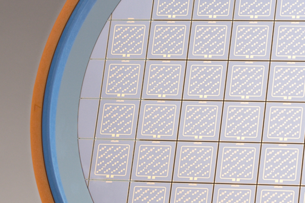
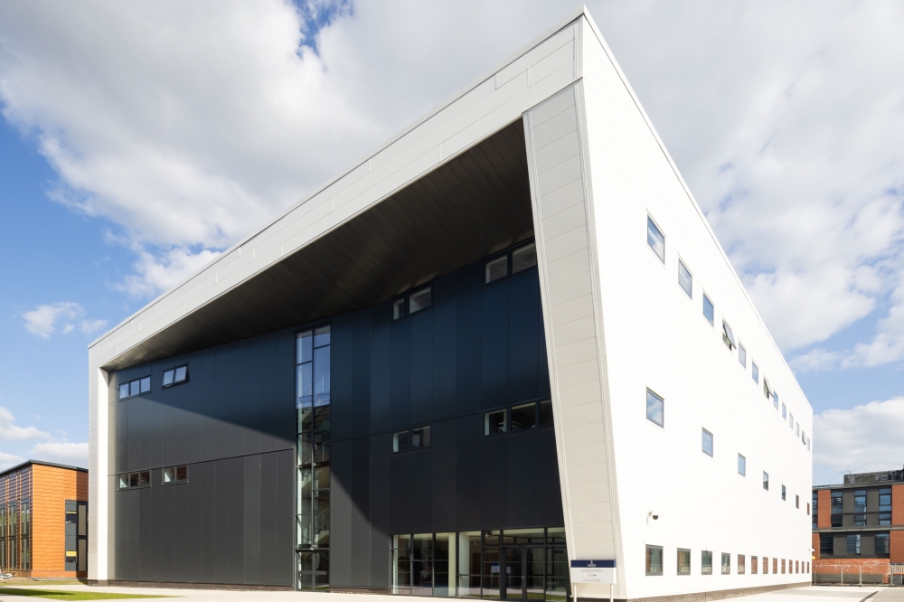
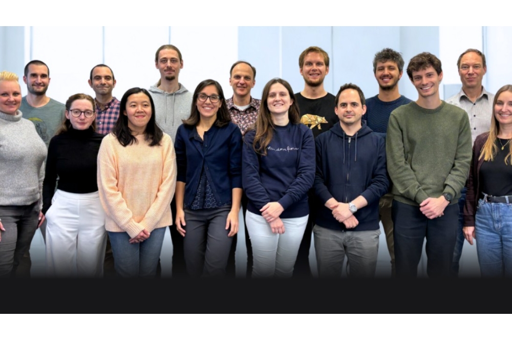
The joint lab, formed in 2004, brings together 120 researchers in the Paris region and actively cooperates with CEA-Leti’s laboratories at Grenoble.
“Our mastery of all the stages of design and manufacture of microelectronic and optoelectronic components as well as their integration into complex devices is an undeniable major asset for our Laboratory”, says Jean-René Bois, chairman and managing director of III-V Lab.
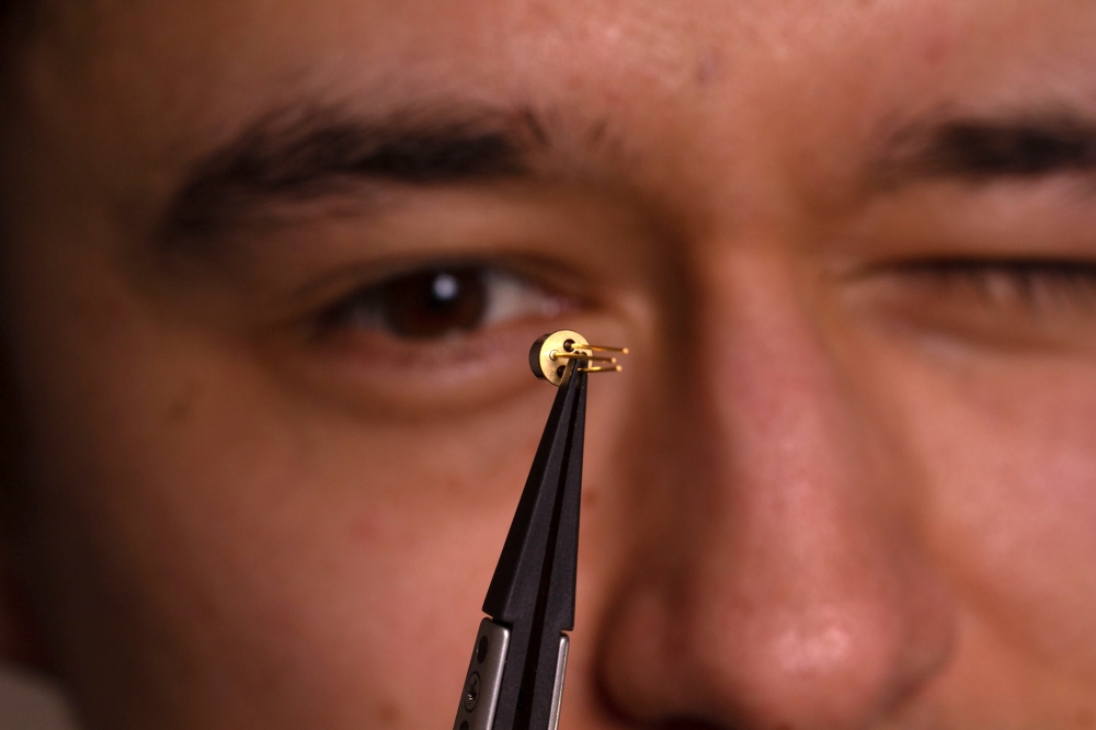
The first mission of III-V Lab is to reach the state-of-the-art in many different domains, and the second mission is to lead utilisation with industrial partners.
For example, these there have been infrared technology transfers to Lynred in 2012, and microelectronics functions to United Monolithic Semiconductors. The Lab has also created the spin-offs MirSense in 2015 and Almae Technologies in 2016.
Furthermore, III-V Lab positioned itself as a key contributor and technology provider of the Pilot Lines of the Horizon Europe framework.
“III-V Lab is a good example of Thales' strategy to master its supply chain for critical and differentiating technologies through strategic partnerships”, explains Bernhard Quendt, CTO of Thales.
III-V Lab says its heritage, and in particular the combination of laboratories and teams from which the company came, was created well before III-V Lab was founded in 2004. But this heritage has been producing an ever more fruitful legacy for its parent companies and its partners, thanks to gathering complementary skill sets and areas of interest under the III-V Lab umbrella. “The passion, the interactive discussions between our experts are key factors of our success!” says Jean-René Bois.
III-V Lab operates i the Paris-Saclay 'Optics valley' and in the Grenoble 'Silicon valley'.
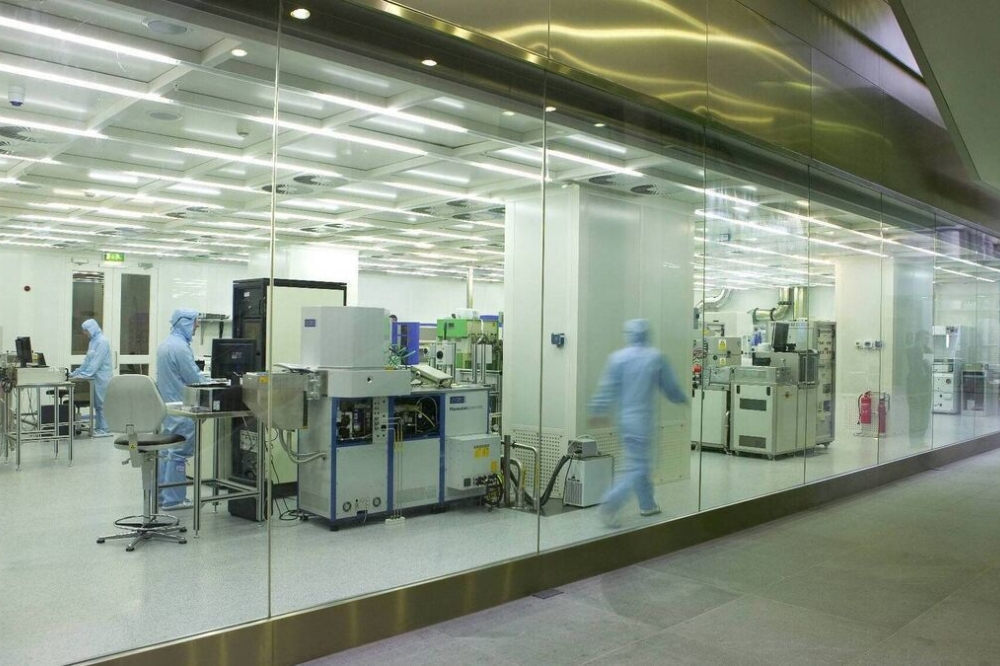
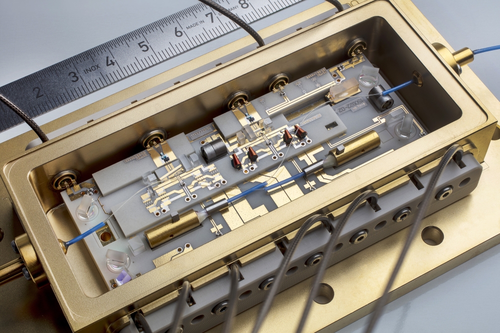
“With complete 200 and 300 mm process lines and up to date foundry equipment, CEA-Leti’s cleanrooms in Grenoble take III-V Lab innovations from lab to fab environment,” says Jean-René Lèqueypes, CTO at CEA-Leti. “With CEA-Leti, III-V Lab can rely on high-end equipment available on 200 and 300 mm for its R&D activities or to demonstrate the scalability of its innovations. CEA-Leti’s know- how in silicon technologies is also a key asset to investigate the integration of III-V semiconductors on Si”.
Peter Vetter, president of Bell Labs Core Research, Nokia, adds “Bell Labs has a rich history of researching semiconductor components, which are essential for differentiating communication systems. The state-of-the-art equipment that we share with Thales and CEA-Leti at III-V Lab has enabled our researchers to realise worldclass optical devices that have been fundamental for our bleeding edge optical network innovations for 20 years.”