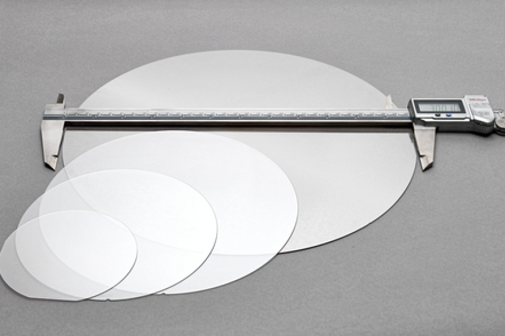
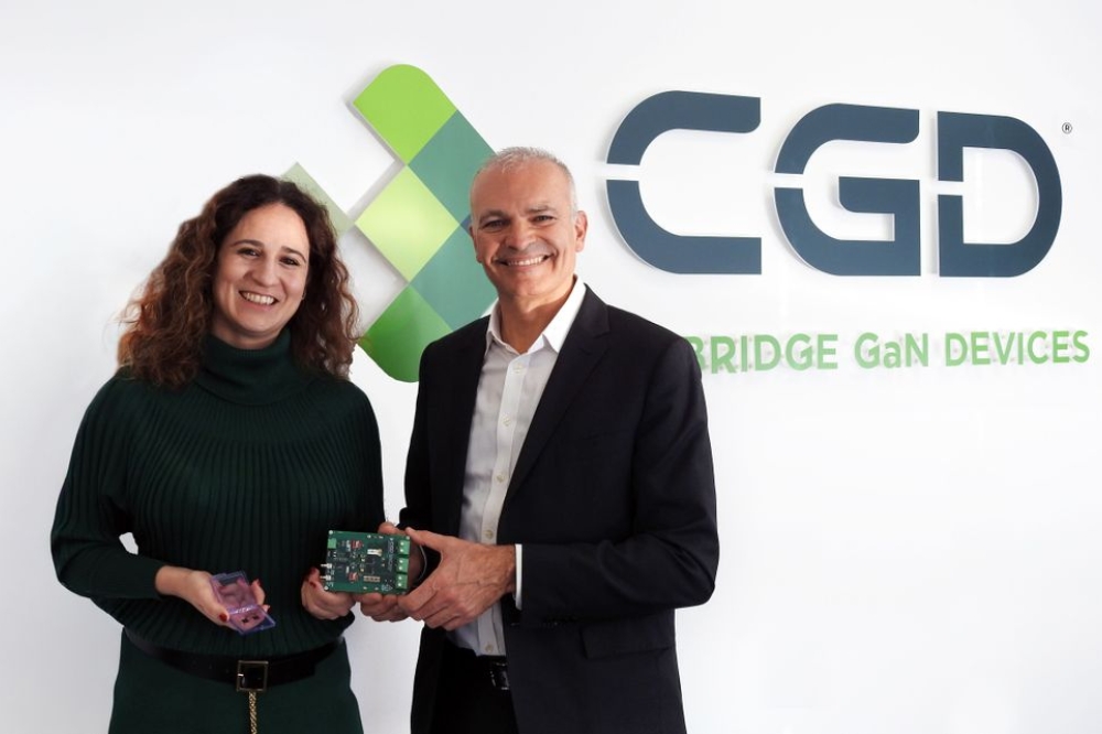
Comptek completes installation of 200mm wafer pilot line
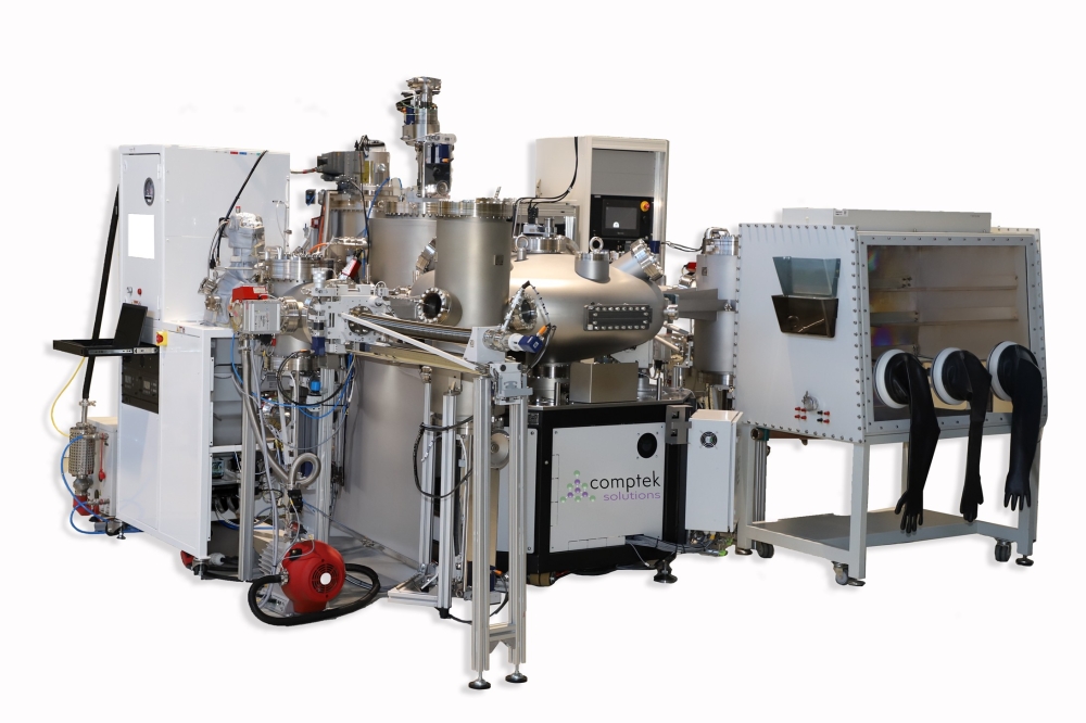
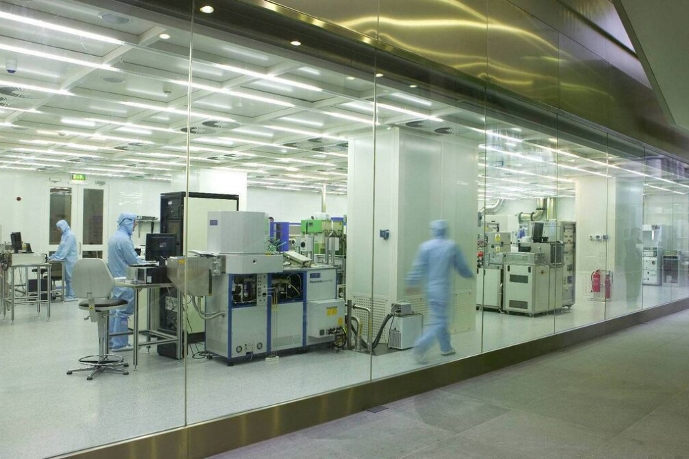
Comptek Solutions, a Finnish maker of advanced passivation technology for the semiconductor industry, has announced the successful design and installation of its pilot line, funded by the European Innovation Council (EIC).
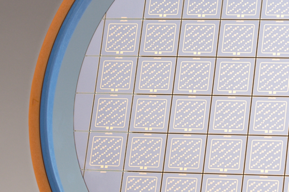
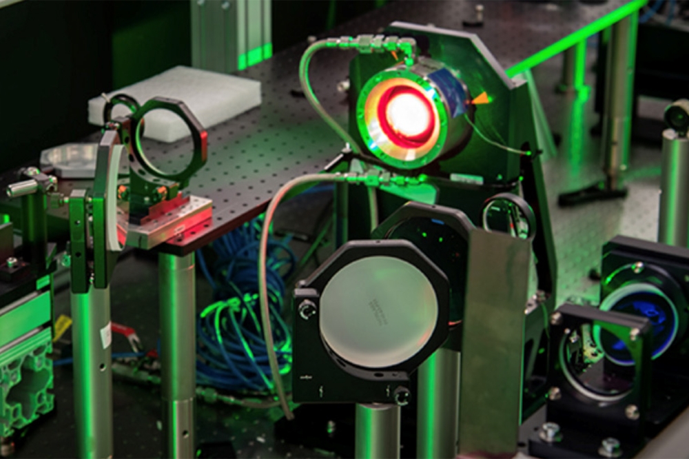
The state-of-the-art pilot line integrates Comptek's proprietary Kontrox passivation technology with other widely used industry techniques such as Atomic Layer Deposition (ALD), delivering a scalable solution for industrial manufacturing for power electronics and optoelectronic applications.
“The pilot line we’ve developed through the EIC-funded 'Enlight' project is a testament to our commitment to pushing the boundaries of passivation technology," said Vicente Calvo Alonso, CEO and co-ounder of Comptek Solutions. "The possibility to combine our unique Kontrox passivation technique with advanced ALD capabilities allows us to deliver highly customisable and optimised solutions, designed to overcome the challenges and fulfill the needs of power electronics and optoelectronic manufacturers. With this pilot line, we are excited to offer our customers the opportunity to tailor the processes to their exact production requirements, helping them achieve unprecedented performance for their device applications."
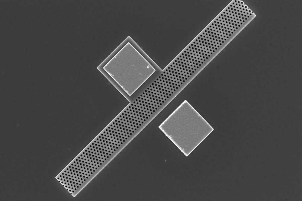
The integration of Comptek’s Kontrox process with ALD technology was implemented using Veeco’s PE-ALD FIJI 200 system. This combination provides a new approach to minimising surface defects and creating a sharp III-V dielectric interface. The result, according to the company, is superior interface quality, crucial for maximising chip performance and optimising yields in a wide range of semiconductor applications, from sidewall passivation layers for µLEDs to complex gate stack dielectrics for power transistors.
Comptek says its EIC-funded pilot line, with its immense potential for next-level compound semiconductor-based substrate passivation, has already attracted significant interest. Several major manufacturers have scheduled trial runs and the company’s capacity for 2025 is already fully booked.