Researchers find way to 'hear' defects in hBN
An international research team led by NYU Tandon School of Engineering and KAIST (Korea Advanced Institute of Science and Technology) has pioneered a new technique to identify and characterise atomic-scale defects in the 2D compound semiconductor hexagonal boron nitride (hBN).
They think this advance could accelerate the development of next-generation electronics and quantum technologies.
The team reported that it was able to detect the presence of individual carbon atoms replacing boron atoms in hBN crystals. This discovery, reported in ACS Nano's October 22, 2024, was made possible by listening to the electronic 'noise' in specially designed transistors, akin to hearing a whisper in a quiet room.
"In this project, we essentially created a stethoscope for 2D materials," said Davood Shahrjerdi, one of the paper's corresponding authors along with Yong-Hoon Kim. "By analysing the tiny and rhythmic fluctuations in electrical current, we can 'perceive' the behaviour of single atomic defects."
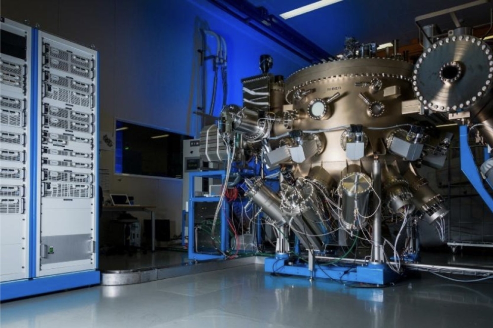
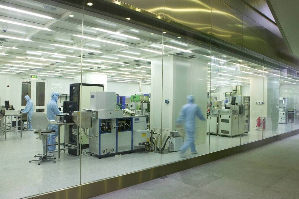
Shahrjerdi is an associate professor in NYU Tandon’s Electrical and Computer Engineering Department, a faculty member of NYU WIRELESS, and the director of the NYU Nanofabrication Cleanroom (NanoFab) that opened in 2023. Kim is professor of Electrical Engineering at KAIST. Shahrjerdi and Kim are also affiliated faculty at NYU-KAIST Global Innovation and Research Institute where they lead collaborations in the NYU-KAIST Next-Gen Semiconductor Devices and Chips research group.
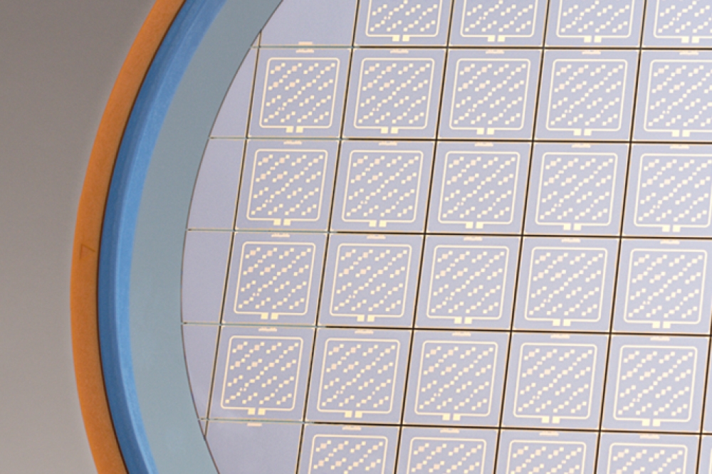
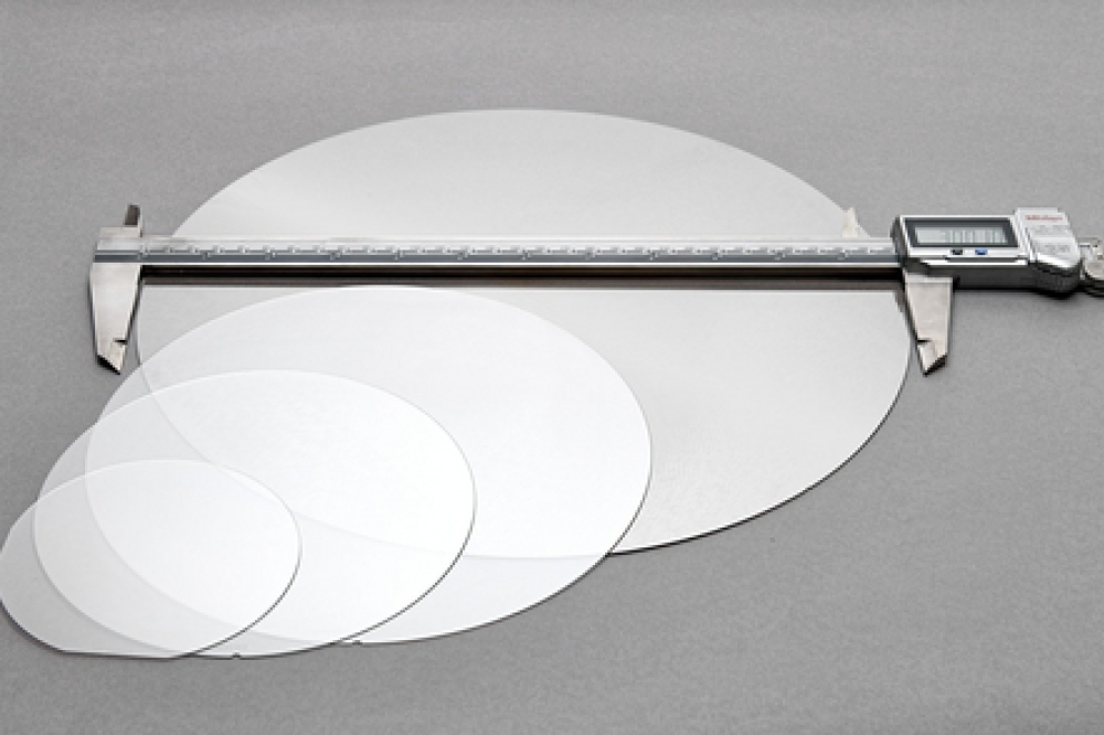
hBN’s atomically thin structure and excellent insulating properties make it an ideal medium for hosting exotic physical phenomena that are not possible with conventional materials. The atomic defects in hBN can degrade its electronic properties, sometimes in ways that could be harnessed for quantum technologies.
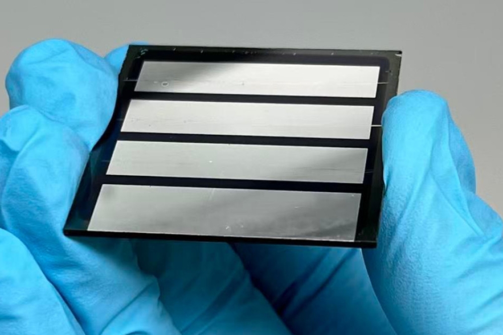
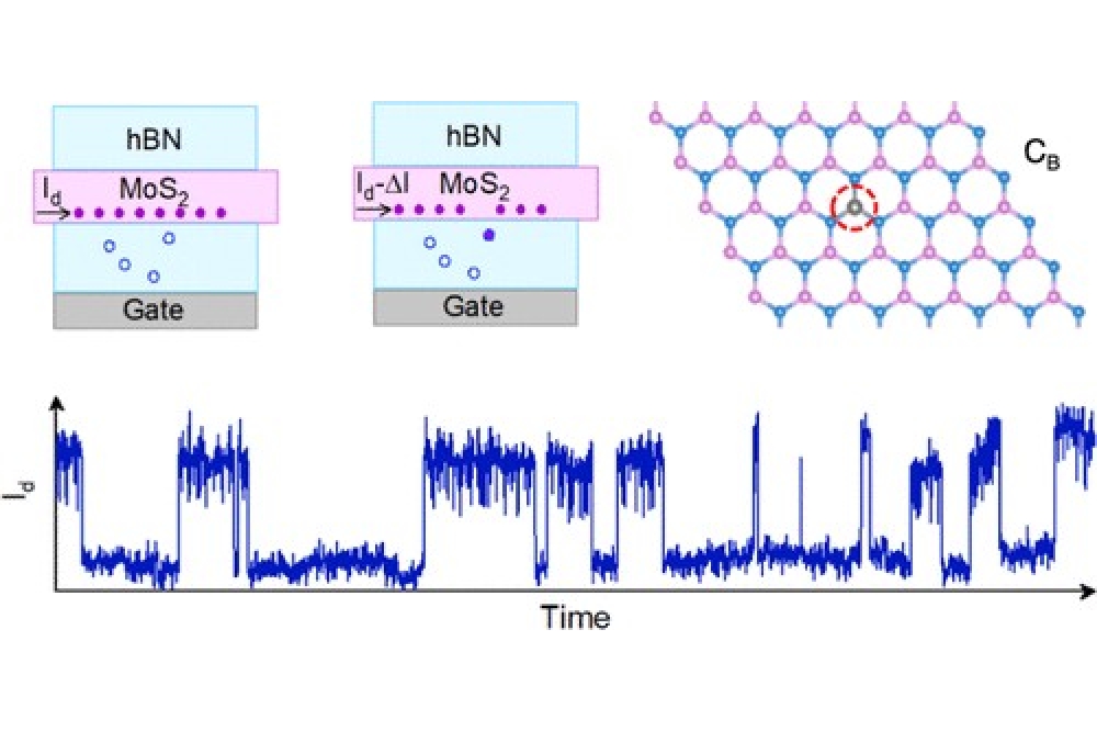
The NYU team built a transistor using 2D MoS2 sandwiched between layers of hBN. By cooling this device to cryogenic temperatures and applying precise electrical voltages, they were able to observe discrete jumps in the current flowing through the transistor.
These jumps, known as random telegraph signals (RTS), occur when electrons are captured and released by defects in the hBN. By carefully analyzing these signals at different temperatures and voltages, the team was able to determine the energy levels and spatial locations of the defects.
"It's like we've developed a microscope that can 'see' individual atoms, but instead of light, we're using electricity," said Zhujun Huang, the paper’s first author who was an NYU Tandon ECE PhD student at the time of the study.
The KAIST team then used advanced computer simulations to clarify the atomistic origins of the experimental observations. Specifically, this combination of experiment and theory revealed that the defects are carbon atoms sitting in places where boron atoms should be in the hBN crystal structure.
"Understanding and controlling the defects in 2D materials could have significant implications for the future of electronics and quantum technologies," explained Sharhrjerdi and Kim. "For example, we might be able to create more perfect quantum material platforms for discovery of new physics or single-photon emitters for secure communications."
In the United States, support for the research came from the National Science Foundation and the US Department of Energy's Center for Functional Nanomaterials at Brookhaven National Laboratory. South Korean contributions included multiple grants from the National Research Foundation of Korea, the BK21 Plus program at KAIST, and computational resources from the KISTI Supercomputing Center. Japanese support was provided by the Japan Society for the Promotion of Science (JSPS) KAKENHI and the World Premier International Research Center Initiative (WPI) of MEXT.