Simulations point the way towards better solar cells
Halide perovskites are a promising material for making more efficient solar cells. Now, researchers at Chalmers University of Technology, in Sweden, have gained new insight into their function, which they've presented in an article 'Impact of Organic Spacers and Dimensionality on Templating of Halide Perovskites' published in ACS Energy Letters.
Halide perovskites absorb and emit light in an extremely efficient way. However, they also degrade quickly, and in order to know how best to apply these materials, a deeper understanding is required of why this happens and how the material functions.
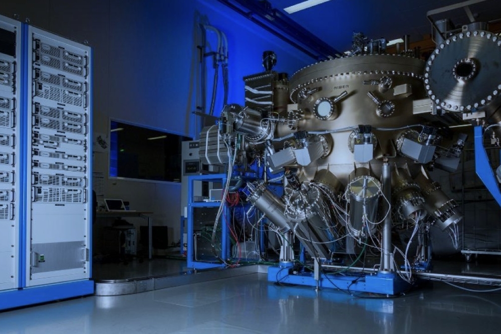
Perovskites come as 3D and 2D materials, the latter often being more stable. Using advanced computer simulations and machine learning, a research team at the Department of Physics at Chalmers University of Technology studied a series of 2D perovskite materials and gained crucial insights into what influences properties.
“By mapping out the material in computer simulations and subjecting it to different scenarios, we can draw conclusions about how the atoms in the material react when exposed to heat, light, and so on. In other words, we now have a microscopic description of the material that is independent of what experiments on the material have shown, but which we can show to lead to the same behaviour as the experiments. The difference between simulations and experiments is that we can observe, at a detailed level, exactly what led to the final measurement points in the experiments. This gives us much greater insight into how 2D perovskites work,” says Paul Erhart, a member of the research team at Chalmers University of Technology.
Using machine learning has been an important approach for the researchers. They have been able to study larger systems, over a longer period, than was previously possible with the standard methods used just a few years ago.
“This has given us both a much broader overview than before, but also the ability to study materials in much more detail. We can see that in these very thin layers of material, each layer behaves differently, and that’s something that is very, very difficult to detect experimentally,” says Julia Wiktor from the research team, which also included researcher Erik Fransson.
Better understanding of the material’s composition
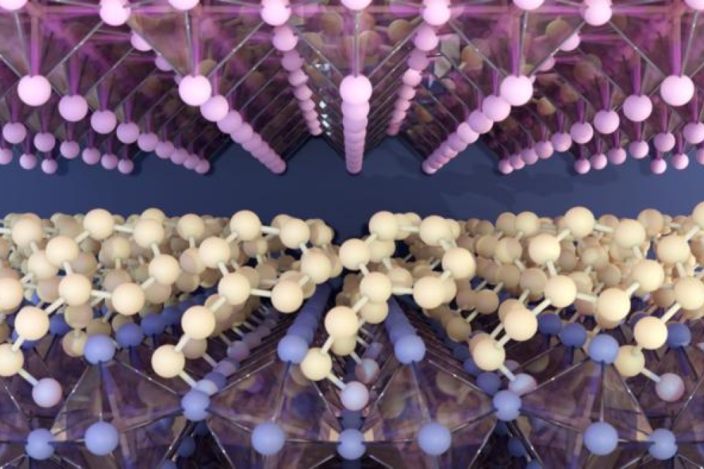
2D perovskite materials consist of inorganic layers stacked on top of each other, separated by organic molecules. Understanding the precise mechanisms that influence the interaction between the layers and these molecules is crucial for designing efficient and stable optoelectronic devices based on perovskite materials.
“In 2D perovskites you have perovskite layers that are linked with organic molecules. What we have discovered is that you can directly control how atoms in the surface layers move through the choice of the organic linkers and how this affects the atomic movements deep inside the perovskite layers. Since that movement is so crucial to the optical properties, it’s like a domino effect,” says Paul Erhart.
The research results provide greater insight into how 2D perovskite materials can be used to design devices for different applications and temperature variations.
“This really gives us an opportunity to understand where stability can come from in 2D perovskite materials, and thus possibly allows us to predict which linkers and dimensions can make the material both more stable and more efficient at the same time. Our next step is to move to even more complex systems and in particular interfaces that are fundamental for the function of devices,” says Julia Wiktor.
The research was supported by the Swedish Research Council, the Chalmers Initiative Advancement of Neutron and Synchrotron Techniques, the Swedish Foundation for Strategic Research, and the Wallenberg Academy Programme. The calculations were made possible by resources from the National Academic Infrastructure for Supercomputing in Sweden (NAISS) at C3SE.