Setting the SiC standard

With its six inch SiC line up and running, the New York Power Electronics Manufacturing Consortium is ready to deliver next generation MOSFETs, reports Rebecca Pool.
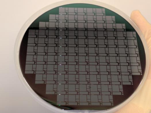
First patterned SiC wafer from the New York Power Electronics Manufacturing Consortium. [NY-PEMC]
In a breakthrough for power MOSFET qualification, the New York Power Electronics Manufacturing Consortium (NY-PEMC), led by the State University of New York Polytechnic Institute (SUNY Poly), recently produced patterned wafers in its SiC process line at SUNY Poly's Albany, NY, campus.
As Dr. Jeffrey C. Hedrick, Vice President of SUNY Poly, tells Compound Semiconductor: "This means we are up and running, our tools are up and running, and our engineers and scientists are now working hard to fabricate these advanced devices."
It all started in 2014, when the General Electric Company (GE) partnered with SUNY Poly to build a state-of-the-art 150 mm process line for silicon carbide MOSFETs and diodes.
Forming the New York Power Electronics Manufacturing Consortium - NY-PEMC - with SUNY Poly, GE provided more than $100 million in intellectual property, while overall investment in the consortium, including support from New York State, reached $500 million.
Then, come 2015 and another $100 million in New York State funds, GE and SUNY Poly revealed plans to establish a power electronics packaging facility at the Computer Chip Commercialization Center (Quad-C) located on SUNY Poly's Utica campus.
And with Danish power module manufacturer, Danfoss Silicon Power, recently joining GE and SUNY Poly to set up SiC power module packaging operations here, NY-PEMC looks set to become the 'silicon carbide corridor' of North America.
Hedrick certainly thinks so. Heading up both the wafer fabrication and packaging arms of NY-PEMC, he highlights how the manufacturing consortium will help provide much needed jobs and revitalise the economy of Upstate New York.
GE will fabricate cutting-edge SiC chips that will then be assembled and packaged by Danfoss for integration into systems. Fabrication capabilities will top 15,000 wafers a year, and with Danfoss earmarked to operate the only domestic high-volume packaging centre in a burgeoning US market, the future for NY-PEMC looks bright.
"GE and Danfoss are our core members, and we expect to add other key partnerships in the near future," says Dr. Hedrick. "We're equipped to easily run 15,000 wafers a year, which is more than sufficient for the next three years, and we have the expansion capabilities to increase this figure to 50,000 when the market ramps up to higher volumes."
Latest developments
In recent months, activities at NY-PEMC's wafer fabrication arm have focused on scaling up its baseline process flow to manufacturing readiness. The process flow includes technology developed at the GE Global Research Center in Niskayuna, New York. And as Hedrick points out: "GE has been continually working with us to transfer technology from its research centre to our line in Albany."
Right now, the wafer fabrication facility is in its final stages of ISO 9001 certification in a SiC-dedicated Class-1 capable cleanroom. All tools, including photolithography, reactive ion etching, metallization, metrology, measurement, in-line electrical test and more, are nearing full installation. And the consortium's team of engineers intends to have the process flow verified and qualified - to automotive AEC-Q101 reliability specifications - by the end of this year.
"We're focusing on process setup and verification right now," explains Hedrick. "But very soon we will be able to fabricate qualified MOSFET devices with unmatched reliability."
Indeed, come 2018, 1.2 kV MOSFET fabrication will be well underway, and this is just the beginning. Hedrick and colleagues intend to offer 1.7 kV MOSFETS shortly thereafter, and then higher voltage devices and integrated circuits by 2020.
What's more, the tools installed in the SiC process line are 200 mm-capable equipment from top-tier manufacturers, and as Hedrick points out, have been 'chucked down' to support 150 mm wafers.
"The industry is currently transitioning to 150 mm substrates and will eventually transition to 200 mm substrates," highlights Dr. Hedrick. "In a few years from now when the 200 mm substrates are technically and economically viable, we will be able to chuck our tools up at a low cost."
"As the market ramps up, we're going to be ready," he adds.
Meanwhile, activities are also well underway at the packaging center at Quad-C in Utica. The site will house manufacturing lines for industrial, transportation, and automotive applications, while additional lines will be devoted to research and development, and prototyping of new modules and power blocks.
"We have a very aggressive schedule to get the packaging facility set up for Danfoss and we are ordering many of the custom tools right now," says Hedrick. "These have a lead time of up to eight months and we'll get many of them by the end of this year."
"We'll start installing these tools as soon as we can, and have the first three lines qualified in 2018," he adds.
So with all systems go for the next few years, what does the longer-term hold for NY-PEMC? Hedrick, for one, hopes to continue extending what he describes as the power electronics ecosystem within NY-PEMC.
"I'm currently seeking additional funding to create a design centre for power electronics devices and systems," he says. "We're also very open to working with businesses that may want to bring SiC substrate and epi wafer production capability to New York. We'll continue to develop this high-tech corridor across New York, and I expect that many consumable and equipment suppliers will soon be joining us."


