Developing efficient, reliable UV LEDs
The performance of the UV LED improves by trimming its dislocation density, boosting light extraction and enhancing thermal management BY NEYSHA LOBO PLOCH FROM UV PHOTONICS AND FBH, AND MICHAEL KNEISSL FROM TU BERLIN AND FBH
Sales of the UV LED are rising, as more devices are being deployed in applications ranging from the disinfection of water, air and surfaces to medical diagnostics, phototherapy, and the curing of various materials. The success of this device is driven by its superior attributes to the incumbent source, the mercury lamp. The UV LED can be turned on and off in an instant, it doesn’t run hot, it is environmentally friendly, radiation hard, and its emission spectra can be selected to cover almost anywhere in the UVA, UVB and UVC range. What’s more, it has a low operating voltage, a compact size and it is robust, making it ideal for portable, battery powered applications.
Despite all these strengths, sales revenue for the UV LED is still dwarfed by that for the mercury lamp. That’s partly because fabrication technologies for this class of device are still at an early stage, and large-scale manufacturing is yet to take place.
There are also other issues, related to performance. Conversion efficiency for the UV LED is far lower than that for its blue cousins and is below ten percent in the UVB and UVC. And lifetime is far shorter: UVC LEDs may last for only a few thousand hours, or even a few hundred. These weaknesses crank up costs associated with ownership and maintenance, and are a barrier to a commercially successful, widely deployed technology.
To improve the commercial viability of the UV LED, there needs to be improvement in the lifetime, wall-plug efficiency and external quantum efficiency. The good news is that for the most part, values for these characteristics are not held back by fundamental physical limitations but can be increased by refining the fabrication technology.
Developing efficient devices
At UVphotonics, working in partnership with the Joint Lab GaN Optoelectronics that has been established between Technische Universität Berlin (TU Berlin) and Ferdinand-Braun-Institut (FBH), we are trying to address these key weaknesses of the UV LED. Our efforts are focused on increasing the efficiency and reliability of devices that are grown by MOCVD and emit in the UVB and UVC. The devices that we have made span 340 nm to 218 nm (see Figure 1).
To drive the development of devices that are cheaper, more powerful and longer lasting, we are evaluating and optimising each step of the LED fabrication chain, from growth of the different semiconductor layers with varying material compositions that make up the LED heterostructure to the packaging of the individual chips.
The first decision facing any maker of UV LEDs is the choice of substrate. We have chosen sapphire: it is optically transparent, low in cost and available in diameters up to 8 inches.
Sapphire’s weakness is that it has a large lattice mismatch with the AlGaN layers of the UV LED. This results in threading dislocations, generated at the interface during growth. If these defects propagate to the active region, where light is generated, they act as non-radiative recombination centres, pegging back device efficiency. According to simulations and experiments, this influence is so severe that the output power of 280 nm LEDs can more than halve when the threading dislocation density increases from 1 x 109 cm-2 to 5 x 109 cm-2.
To reduce the detrimental effects of threading dislocations in our UVB LEDs, we use thick AlN layers, followed by a strain management section, made of alternating thin layers of GaN and AlN. With this approach, the threading dislocation density is about 3 x 109 cm-2.
At even shorter wavelengths, dislocations are even more detrimental to efficiency. To combat this, fabrication of our UVC LEDs begins with epitaxial lateral overgrowth, to reduce the threading dislocation density down to around 1 x 109 cm-2.
We are currently investigating other promising, cost-effective techniques to reduce the threading dislocation density. They include sputtering AlN on sapphire, followed by annealing at high temperatures, to obtain a high-quality crystalline layer.
The growth of our UV LED structure begins with the silicon-doped n-type AlGaN layer, which must combine transparency at the emission wavelength with high electrical conductivity for homogeneous lateral current-spreading. After this is the active region, containing several AlGaN or InAlGaN quantum wells, followed by an electron-blocking layer that prevents electrons from escaping out of the active region, and a highly conductive magnesium-doped p-type AlGaN layer for hole injection.
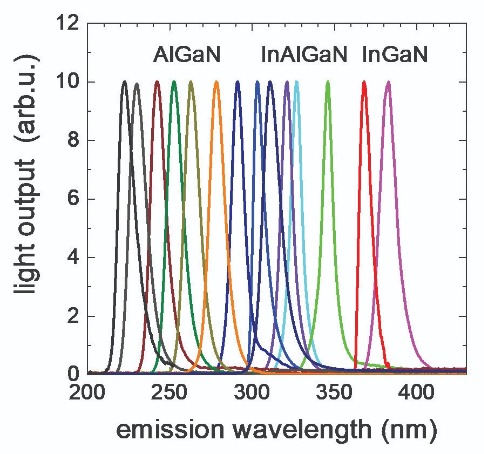
Figure 1. Normalized emission spectra of III-nitride based UV LEDs fabricated within the Joint Lab GaN Optoelectronics between TU Berlin and FBH Berlin. © TU Berlin
These LED epiwafers are processed into lateral geometry devices using standard lithography techniques. A laser scribing and dicing process follows, to create individual die. Using this approach, we have produced 310 nm UVB LEDs with a 30 mW output at 350 mA. After burn-in, the extrapolated lifetime – evaluated in terms of the time taken for the output power to halve – is 8,000 hours.
As expected, moving to shorter wavelengths reduces the output: at 265 nm, which is in the UVC, our devices deliver a 25 mW output at 350 mA. At the even shorter wavelength of 233 nm the output is just 0.3 mW at 100 mA. Note that this result is obtained for one of the first fully packaged UVC LEDs worldwide to produce a single emission peak at such a short wavelength.
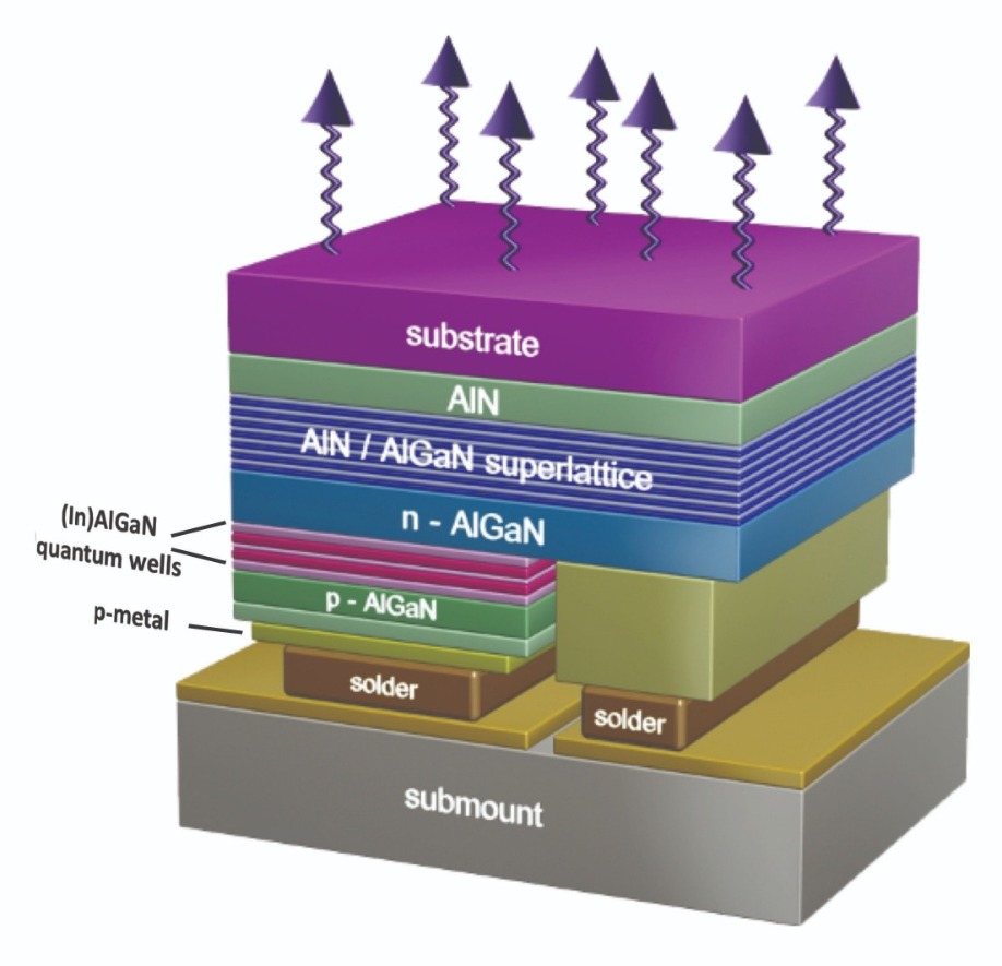
Figure 2. A flip-chip mounted III-nitride based UV LED die. © TU Berlin
Getting the light out
In every LED, not all of the light that is generated within the active region exits the chip. But this situation is more severe in UV LEDs, as the high refractive index of the AlGaN layers increases the total internal reflection, leading to a hike in the absorption of UV light within the device. In particular, light is lost at the metal contacts and the p-AlGaN hole-injection layers.
Another issue with UV LEDs is that light extraction is influenced by changes in the valence band structure of the group III-nitrides. As the emission wavelength decreases – due to increases in the aluminium content in the quantum wells – the polarization of the emitted light changes. At longer wavelengths, emission is mainly transverse electric polarized with respect to the surface normal of the (0001) c-plane oriented sapphire substrate, but as emission heads deeper into the UV, polarization becomes predominantly transverse magnetic. This orientation leads to a lower light extraction from the chip.
According to extensive experimental and theoretical studies, the switch from transverse electric to transverse magnetic takes place at around 240 nm. However, this crossover point can be shifted by changes to the substrate orientation, and to the strain and confinement within the quantum wells.
For a typical UVB LED that is not equipped with any light extraction features, simulations suggest that just 8 percent of the light that is generated in the active region exits the chip. And at shorter wavelengths, this figure is even less. Consequently, light extracting technologies are essential for realising high-efficiency devices.
Our team is developing two approaches to boost light extraction: p-transparent current spreading layers, combined with a reflective low-resistant p-metal contact, such as a transparent ITO layer together with an aluminium reflector; and growth on patterned sapphire substrates. With the latter, light extraction efficiency rises via an increase in the direct extraction of light and a randomisation of the angular distribution of the photons in the LED.
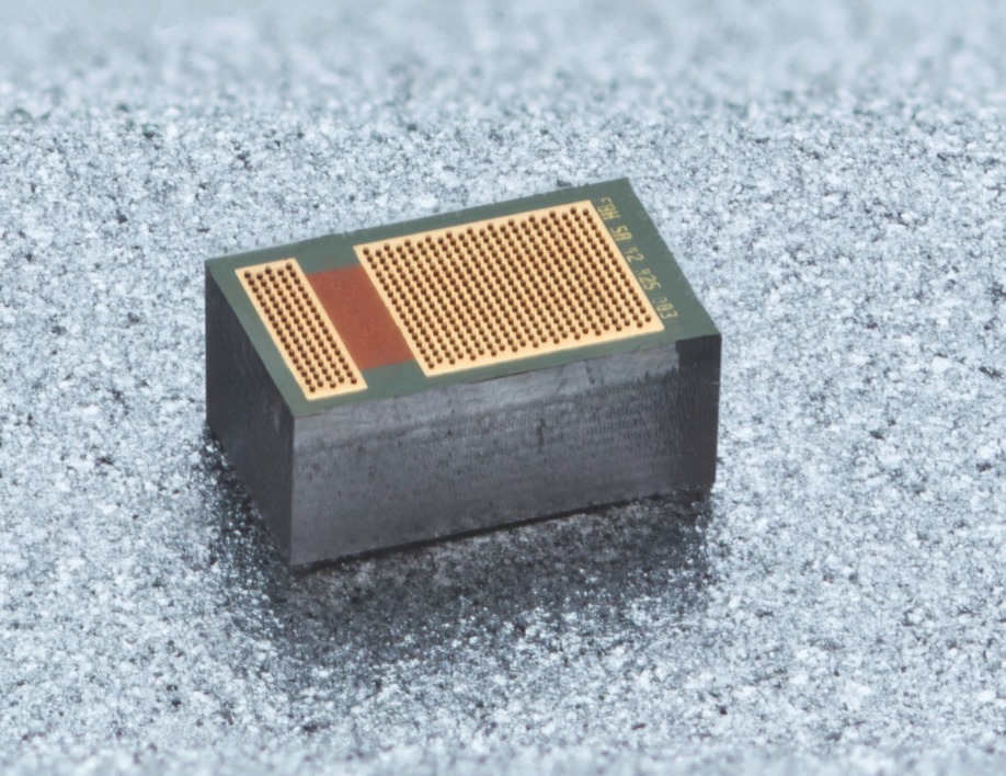
Figure 3. Single UVB LED chip with gold stud-bumps deposited by electroplating at the wafer level. © FBH /schurian.com
The packaging bottleneck
Downsides of low wall-plug efficiencies are not limited to a low output power. With less light getting out, more heat is generated within the chip. That’s a big issue, as higher temperatures impair the electrical and optical characteristics of the LED, and also speed its degradation.
The most common approach to prevent an UV LED chip from overheating is to flip-chip bond the low thermal conductivity sapphire die to a material that can suck the heat away. With this approach, the die is bonded epi-side down, enabling heat to transfer efficiently to the metal bonding pads (see Figure 2).
It would be a mistake to combine this flip-chip device with inexpensive, readily available alumina ceramic packages that are commonly used for visible LEDs and have a limited thermal conductivity. Far better is one of the newer packages being developed for deep UV LEDs that feature AlN ceramic layers with thermal conductivities of 150-170 W m-1 K-1.
These packages are far from ideal, though. As well as being pricey – they are more than a dollar a piece – it is difficult to integrate them with an aluminium UV reflector. In addition, device encapsulation is tricky, as the majority of state of the art, high-index transparent silicones and epoxy resins that are used in visible LEDs are not stable when exposed to high-energy UV photons.
Given these issues, today’s packaged deep-UV LEDs tend to include UV transparent quartz windows or lenses. This adds to the price, and can increase the complexity of manufacturing, because integrating quartz lenses into the device is challenging. Clearly, the development of inexpensive packaging materials for deep-UV LEDs is pivotal to commercial viability.
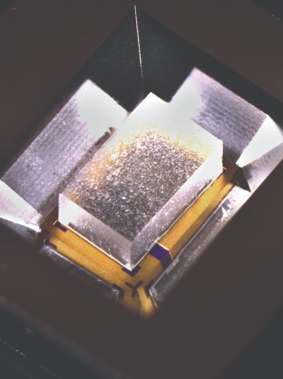
Figure 4. 320 nm LED flip-chip mounted in a silicon package. The package is developed by the CiS Research Institute forMicrosensors, Germany © CiS
We are trying to address all these issues associated with thermal management. Our approach involves using thermocompression bonding of gold stud bumps for the first interconnect between the chip and the package. We use electroplating to deposit, directly on the LED wafer, a hexagonal array of 15 mm-wide, 8 mm-high stud bumps, separated by a pitch of 30 mm (see Figure 3). Thanks to gold’s thermal conductivity of 320 W m-1 K-1, simulations suggest that the thermal resistance of this interconnect can be as low as 7.15 K W-1 for 320 nm LEDs with a 20 percent coverage by studs on the metal pads. Note that we can use our electroplating process to produce uniform deposition of gold studs across a complete 2-inch wafer, and this can be extended to far larger wafers to trim costs.
In collaboration with our partners at the CiS Research Institute for Microsensors, we are developing a silicon-based package for UV LEDs (see Figure 4). Drawing on our collaborator’s great expertise in silicon technology, we are able to develop a cost-effective package that combines a low thermal resistance with the integration of versatile features, such as an aluminium reflector for increased light extraction, integrated diodes to prevent electrostatic damage, and monitoring sensors.
What’s next?
The UV market is definitely on the up, with ever more companies competing for sales. There is tremendous acceleration in the pace of development of UVB and UVC LEDs, and in the coming years, the focus will be on the development of advanced technologies to increase light extraction and on cost-effective packages exceling in thermal management.
Two of the biggest issues are arguably lifetime and the cost-per-watt. A far longer lifetime is needed to ensure stability of the UV LED systems for real world applications. Meanwhile, while today’s bang-per-buck of around $1 per milliwatt might be good enough for early adopters, breaking into the mass market will require a seismic shift to around $1 per watt for devices delivering far longer lifetimes.


