
b-Ga2O3 The next chapter

Speeding MOCVD growth sets the stage for device development by Ross Miller, Fikadu Alema and Andrei Osinsky from Agnitron Technology
Gallium oxide is a very promising material for making power and optoelectronic devices. It has a great set of intrinsic properties, and preliminary device testing indicates that it could have the upperhand over SiC and GaN power devices in high-voltage switching. What's more, it has the potential to produce highperformance solar-blind UV photodetectors.
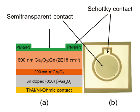
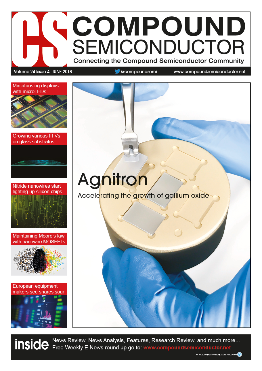
Figure 1. (a) Crosssectional view of the photodiodes based on a β-Ga2O3:Ge homoepitaxial film grown by MBE on the bulk n+ β-Ga2O3 substrate. (b) Optical image showing the top view of the vertical Schottky photodiode.
This ultra-wide band gap material comes in five different flavours. The most promising is the monoclinic polymorph β-Ga2O3. It has the unique combination of a very large bandgap energy "“ it is 4.9 eV "“ and a conductivity that can be varied over a vast range, due to doping control that extends from 1 x 1015 cm-3 to 1 x 1020 cm-3. Armed with these attributes, β-Ga2O3 can withstand electric fields that could cause failure in SiC and GaN.
Holding back progress with β-Ga2O3-based devices are weaknesses associated with the growth of its epilayers. Drawbacks with MOCVD, MBE and HVPE are preventing the rapid deposition of thick films of β-Ga2O3 and its related alloys with properties needed to underpin the commercialisation of power devices and photodetectors.
But these issues are not insurmountable, according to our work at Agnitron Technology of Eden Prairie, MN. Our efforts have shown that with the right approach, MOCVD has been demonstrated to support growth rates up to 10 μm/hr, which is more than an order of magnitude higher than previously; far higher electron mobilities than before; and complementary AlGaO alloys with an aluminium content of more than 40 percent.
Native substrates
Another appeal of β-Ga2O3-based technology is that native substrates are available and can enable growth of high-quality epilayers without special techniques required when epilayers and substrates are crystal lattice mismatched. This foundation can be produced by several techniques, including edge-defined film-fed growth and the Czochralski technique.
One tremendous advantage of being able to produce native substrates is that it enables the growth of lowdefect-density epitaxial films. These are a prerequisite for producing power electronics devices with a high critical electric field strength as defects are a primary cause for device breakdown at lower than expected fields.
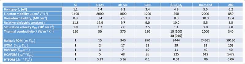
Table 1. Comparison of various semiconductor material properties as well as several key figures of merit (taken from the last two papers listed in Further reading). Commercial development of β-Ga2O3 devices will have to consider thermal management and packaging R&D, due to the relatively low thermal conductivity of this oxide.
In addition, melt techniques "“ and specifically the Czochralski technique that is used to make countless silicon substrates "“ have already realised low material costs by scaling up production. Assuming sufficient demand, one should expect that costs for β-Ga2O3 substrates can asymptotically approach cost parity with those for silicon and sapphire.
Note that the road to commercialisation for β-Ga2O3 is markedly different to that for SiC and GaN. Both those materials have far better material properties for high-voltage operation than those of silicon, but have faced manufacturing challenges, due to various issues related to substrates and processes. This leaves the door ajar for alternative material systems, including Ga2O3, which is not hampered by those weaknesses and may offer differentiated performance for some applications.
Our initial involvement with β-Ga2O3 was not associated with power devices, but with UVC photodetectors. Working in partnership with researchers at the University of California, Santa Barbara (UCSB), and the University of Central Florida (UCF), we fabricated Schottky photodiodes with this material system.
Despite a lack of optimisation, these detectors exhibited a high photoresponsivity and a high rejection ratio (see Figures 1 and 2). We believe that further effort, enabling a tuning of the energy gap and cut-off wavelength by bandgap engineering via compositional tuning of β-(AlGaIn)2O3 alloys, could lead to the commercialisation of true solar-blind, full UV spectrum detectors.
Figure 2. (a) Current-time characteristics of the vertical Schottky device based on β-Ga2O3: Ge epitaxial film from Figure 1 under dark and illuminated conditions. (b) Spectral response of the Pt-β-Ga2O3:Ge vertical Schottky photodiode. (c) Comparison of the photoresponsivity of the non-optimized β-Ga2O3: Ge photodiode (magenta) with commercial devices based on GaN (black), SiC (red) and AlGaN (blue) wide bandgap semiconductors. Estimated quantum efficiency is represented by the dashed lines.
There is no doubt, however, that β-Ga2O3 is attracting the greatest interest as a material for making power electronics. Offsetting its many strengths is that, like other oxide semiconductors, realising a usable p-type doping in this material is elusive "“ and this might always be so.

Glow from oxide heater assembly during burn-in reflects out of the multiwafer MOCVD chamber while open to atmosphere at Agnitron's MOCVD Lab.
However, due to its ultra-wide bandgap and controllable n-type doping over a vast range, there is much interest in developing unipolar devices with vertical and lateral conducting topologies for switching and RF device applications. Progress to date for demonstration of over 1 kV vertical devices includes Schottky diodes, reported in 2017 by a team from NICT in Japan as well as FETs recently by Cornell University "“ and far greater success could follow, as the great intrinsic properties of β-Ga2O3 put realisation of vertical geometry devices with switching voltages exceeding 10 kV on the horizon. Recent demonstration of high mobility two-dimensional electron gas (2DEG) in β-Ga2O3 based heterostructures by Ohio State University and Air Force Research Laboratory also indicates a path to devices which may exceed the voltage performance of GaN HEMTs.
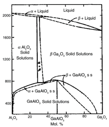
Figure 3. The phase diagram of Ga2O3 and Al2O3. [Hill et al. J. Am. Cer. Soc. 35 135 (1952)]. Solubility of Al2O3 in β-Ga2O3 is drastically reduced below 800°C by formation of the GaAlO3 intermediate compound. MBE growth temperatures are limited to around 600-700 °C due to decomposition of Ga2O3 to volatile sub-oxides. Thus, in MBE growth, the maximum Al2O3 content in β-Ga2O3 is around 20 percent. In contrast, MOCVD growth over 800 °C would facilitate growth above the solid phase congruent point and would allow up to about 60 percent Al2O3 content in the β-Ga2O3 phase.
Epitaxial growth challenges"¦
For high-power β-Ga2O3-based diodes and transistors operating in the kilovolt range, epilayers with a thickness of typically 10 μm or more are needed. Growth rates for MBE are only hundreds of nanometres per hour, ruling out this approach.
The low growth rate is not the only issue, however. Power devices also require layers of the alloy (AlxGa1-x)2O3, in order to form a two-dimensional electron gas. Studying the phase diagrams for Al2O3-Ga2O3 reveals that it is challenging to achieve the temperatures and pressures required for growth of aluminium-rich (AlxGa1-x)2O3 alloys (see Figure 3).
Prior to our work, many limitations also plagued MOCVD. Its growth rate for β-Ga2O3 could not exceed 500 nm/hr; doping concentration was limited, and could not drop below 1 x 1017 cm-3; electron mobilities lagged behind theoretical levels, and those demonstrated by MBE; and the composition of (AlxGa1-x)2O3 was limited, and its doping challenging.
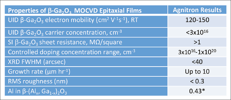
Table 2. Summary of various β-Ga2O3 material parameters illustrating recent advances for β-Ga2O3 MOCVD growth processes. *The result indicates incorporation of an aluminium mole fraction of 0.43 can be achieved in an β-(AlxGa1-x)O3 alloy grown by MOCVD.
"¦ and breakthroughs
Our overcoming of all these limitations can be traced back to our involvement in a two-year STTR programme sponsored by the Army Research Office. In the latter part of this effort, we were tasked with finding a suitable buffer layer for enhancing the performance of solar-blind, MgZnO-based photodetectors. Up until that point, ZnO had been used as a buffer on sapphire "“ but this limited device performance, by tending to absorb incident radiation at longer wavelengths than that of the MgZnO films.
The remedy, recommended by acting ARO programme monitor Michael Gerhold, involved a switch to β-Ga2O3, in the form of either a substrate or buffer material. Through the course of investigating this material, we became acutely aware of MOCVD growth limitations.
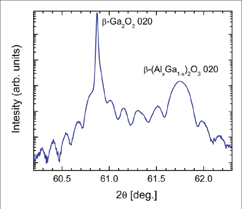
Figure 4. XRD ω-2θ scan profile of a strained β-(Al0.21Ga0.79)2O3/Ga2O3 heterostructure grown on a (010) b-Ga2O3 substrate by MOCVD. The β-(Al0.21Ga0.79)2O3 layer is 70 nm thick.
Following the completion of this project, we embarked on a programme sponsored by the Office of Naval Research (ONR) that focused on increasing the growth rate of MOCVD-grown β-Ga2O3. Success would aid the development of high-voltage power electronic devices, which could be used on military vessels for weapon and transportation systems, such as rail guns, as also for air and missile defence radar and propulsion.
We have made major strides in this latest STTR programme, involving UCSB, and through this effort we have been able to increase the growth rate to 10 μm/hr. Success is not realised by simply increasing the flow of precursors. Although this helps a little, it doesn't address the limiting factor. The difficulty with the growth of Ga2O3 is that when metal organic precursors are injected into the oxygen-rich environment of the growth chamber, they react rapidly in the gas phase, impairing precursor efficiency and ultimately applying the brakes to the growth rate. Our solution is to optimize the pressure and growth temperature, and combine this with a close injection showerhead design that reduces the time that the process gases are mixed, prior to reaching the growth surface. Thanks to this, there is an increase in the number of active precursor species reaching the growth surface, leading to a hike in both the precursor efficiency and the growth rate.
An increase in the growth rate of β-Ga2O3 must go hand-in-hand with other improvements in MOCVD growth technology for this ultra-wide bandgap oxide. Advances must also be made in the range of dopant concentrations, and in realising low background concentrations, a high carrier mobility, a smooth surface morphology and high aluminium content β-(AlxGa1-x)2O3 alloys. We have succeeded on all these fronts (see Table 2 for details).
Our breakthroughs in the doping of β-Ga2O3 include the use of a new approach. Previous efforts involved either tetraethyl orthosilicate (TEOS) or tri-ethyl tin (TESn), while we have used silane as a source of Silicon. Merits of the latter include its common use in MOCVD production processes, allowing delivery in high and low concentrations that support high and low doping levels "“ the doping range exceeds previous reports by roughly an order of magnitude in both directions.
We have also realised a substantial increase in the electron mobility of epitaxial, undoped bulk films achieving comparable mobility as is observed in the high-quality undoped native substrates "“ about 150 cm2 V-1 s-1. In addition, we have set a benchmark for electron concentrations in MOCVD-grown films "“ our material can have electron concentrations that are more than three times lower than those in any other reports. Yet another encouraging result is that, according to X-ray diffraction scans, our epitaxial film crystal quality is so high that it is limited by the starting native substrate. Taken together, all these experimental results indicate a reduction in carrier compensation and scattering in our material, due to reductions in gallium vacancies, dislocations and point defects.
Another breakthrough is the development of a novel, proprietary process for the growth of highly resistive semi-insulating β-Ga2O3 epitaxial films. Layers of highly resistive semi-insulating β-Ga2O3, which are essential for the fabrication of lateral and vertical conducting power devices, are usually formed by adding deep impurities, such as iron or magnesium. But these additions are far from ideal: as they are highly mobile, they can diffuse to adjacent layers, where they are so detrimental that they hamper device performance.
What's more, when iron and magnesium impurities are introduced into an MOCVD growth chamber they have a "˜memory effect', and special treatment is needed to prevent them from having an unwanted impact on subsequent growths. Our proprietary processes avoids these pitfalls for semi-insulating films, while expanding the range of controllability for n-type doped β-Ga2O3 using a range of precursors, which improves process flexibility.
We have also championed the MOCVD growth of aluminium-rich (AlGa)2O3 alloys, breaking new ground with a ternary with an aluminium content of 43 percent. Note that even higher values should be possible. We have also formed: a high-quality, strained (Al0.21Ga0.79)2O3/Ga2O3 heterostructure, which is a critical building block for various device structures (see Figure 4 for an X-ray diffraction spectra); and a strained β-(Al0.21Ga0.79)2O3/Ga2O3 superlattice with abrupt interfaces (see Figure 5). The latter promises to provide defect/dislocation management during the growth of heterostructures, and could be used to form an active region for multi-channel, laterally conducting devices. The next steps will include further optimisation of controllable, n-type doping in AlGaO alloys, a key ingredient for making devices.
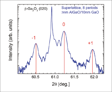
Figure 5. (020) XRD ω-2θ scan for the first β-(Al0.21Ga0.79)2O3/β-Ga2O3 superlattice structure grown by MOCVD at Agnitron Technology. The superlattice structure has 8 periods of β-(Al0.21Ga0.79)2O3/β-Ga2O3, and the thickness of the β-(Al0.21Ga0.79)2O3 barrier and β-Ga2O3 well are 5 nm and 10 nm, respectively. Although this structure is not optimized, observation of Pendellösung fringes in the XRD scan are an indication of surface and crystal qualities. This result represents an important demonstration of MOCVD capabilities.
Another breakthrough is the development of a novel, proprietary process for the growth of highly resistive semi-insulating β-Ga2O3 epitaxial films. Layers of highly resistive semi-insulating β-Ga2O3, which are essential for the fabrication of lateral and vertical conducting power devices, are usually formed by adding deep impurities, such as iron or magnesium. But these additions are far from ideal: as they are highly mobile, they can diffuse to adjacent layers, where they are so detrimental that they hamper device performance.
What's more, when iron and magnesium impurities are introduced into an MOCVD growth chamber they have a "˜memory effect', and special treatment is needed to prevent them from having an unwanted impact on subsequent growths. Our proprietary processes avoids these pitfalls for semi-insulating films, while expanding the range of controllability for n-type doped β-Ga2O3 using a range of precursors, which improves process flexibility.
We have also championed the MOCVD growth of aluminium-rich (AlGa)2O3 alloys, breaking new ground with a ternary with an aluminium content of 43 percent. Note that even higher values should be possible. We have also formed: a high-quality, strained (Al0.21Ga0.79)2O3/Ga2O3 heterostructure, which is a critical building block for various device structures (see Figure 4 for an X-ray diffraction spectra); and a strained β-(Al0.21Ga0.79)2O3/Ga2O3 superlattice with abrupt interfaces (see Figure 5). The latter promises to provide defect/dislocation management during the growth of heterostructures, and could be used to form an active region for multi-channel, laterally conducting devices. The next steps will include further optimisation of controllable, n-type doping in AlGaO alloys, a key ingredient for making devices.
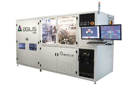
Figure 6. Agnitron's Agilis MOCVD system in a dual-chamber configuration. The β-Ga2O3 configuration is currently available with single chamber designs and specifications noted in Table 3.
The successes we have had will enhance the foundation for upcoming device development. We believe that by optimising the MOCVD process, β-Ga2O3 and its related alloys can be achieved with properties to enable fabrication of devices which encroach theoretically predicted performance. Growth rates are now high enough for commercial device production, but they need to be realised in far larger multi-wafer platforms delivering sufficient throughput of high-quality epitaxial material.
There is good reason to believe that this is possible. History attests to the success of the MOCVD platform for highvolume manufacture of LEDs, laser diodes, and power devices. This growth technique also offers wide process windows and an expansive set of precursors, equipping engineers with the levers they need to optimise selective regrowth, alloying, doping, compensation control, growth rates and gas phase reactions. However, even though MOCVD is a proven success for high-volume manufacturing of nitrides, phosphides and arsenides, it doesn't follow that it's a sure bet for β-Ga2O3. Oxide MOCVD growth has its own unique set of process-related challenges, and they must be addressed if the commercial production of devices based on β-Ga2O3 is to take off.
If a device is to be a commercial success, then the costs associated with epitaxial growth must be modest. After all, that's been the case for other compound semiconductor device types, including LEDs, so one can logically assume that it would be the same for β-Ga2O3 based devices.
One major factor in favour of β-Ga2O3 is that native substrates can be produced by volume scalable bulk growth techniques. This promises a simpler growth process than that for GaN. With SiC, homoepitaxial growth is used, but the substrates are pricey, so it is feasible that the production costs for β-Ga2O3-based devices could even undercut those for SiC and GaN, if volumes were high enough.
To support the commercialisation of β-Ga2O3, we have been working with UCSB to improve MOCVD growth technology associated with this oxide. Efforts began with extensive flow and chemical modelling to identify ideal precursor candidates and establish growth condition windows. This work also helped with the reactor design.
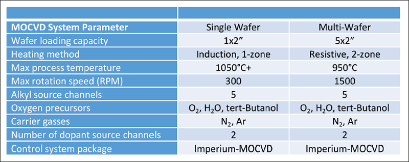
Table 3. System specification for the new Agilis β-Ga2O3 Configuration MOCVD system from Agnitron. Specifications refer to the standard system configuration; some parameters are customizable or expandable.
We are now on our fourth and fifth generations of reactor configurations for the growth of β-Ga2O3. These latest configurations, featuring improved gas injection, are capable of providing process conditions required to achieve world-class β-Ga2O3 material growth.
Using this configuration, we have recently added a tool to our portfolio of Agilis Series R&D MOCVD Systems (see Figure 6). This system is available with single and multi-wafer reactor geometries, and initial customer orders are scheduled for Q3 delivery.
The release of this tool will help to spur the development of β-Ga2O3 optoelectronic and power applications. But there is much work still to do. The multi-wafer configurations are small, and must be scaled while maintaining material quality, in order to trim epitaxial costs. In addition, while it is clear that wide bandgap devices are destined to improve the energy efficiency in electric vehicles, data centres and distributed energy resources, there is still uncertainty over the role that will be played by the various wide bandgap devices. What are the best opportunities for β-Ga2O3, and where can GaN and SiC shine?
The works identified in this article were in large part funded by: ONR contract number N6833518C0192, under the direction of Mr. Lynn Peterson; AFOSR contract number FA9550-17-P-0029, under the direction of Dr. Ali Sayir; and ARO contract number W911NF-14-C-0157, under the direction of Dr. Michael Gerhold. Agnitron also acknowledges Professors James Speck and Winston Schoenfeld for their support and collaborative contributions which have been important to β-Ga2O3 related progress for the Agnitron team.
Further reading
K. Konishi et al. Appl. Phys. Lett. 110 103506 (2017)
Z. Hu et al. Enhancement-mode Ga2O3 vertical Transistors with breakdown voltage > 1 kV, IEEE Electron Device Letters, Early Access, 25 April 2018.
M. Baldini et al. ECS J. Solid State Sci. Technol. 6 Q3040 (2016)
G. Jessen et al. Compound Semiconductor Integrated Circuit Symposium (CSICS), IEEE, Maimi, FL, USA, 2017
M. Higashiwaki et al. physica status solidi (a) 211 21 (2014)
Y. Zhang et al. Appl. Phys. Lett. 112 173502 (2018)


