

Creating commercially viable diamond substrates
Diamond is set to serve in many more high-end applications, thanks to the development of a heteroepitaxial growth process for fabricating 2-inch substrates.
BY SEONG-WOO KIM AND KOJI KOYAMA FROM ORBRAY COMPANY (FORMERLY ADAMANT NAMIKI PRECISION JEWEL)
Crystalline diamond is the ultimate semiconductor. It combines an outstanding degree of crystallinity with an extremely high breakdown voltage, excellent electrical properties and exceptionally high thermal conductivity (see Table 1). Once this allotrope of carbon is put to practical use, it will enable devices that are vastly superior to those incorporating currently available materials, setting far higher benchmarks for voltages, output powers, and efficiencies. What’s more, thanks to the nitrogen vacancy centre that’s unique to diamond, this material has tremendous promise for making sensors.

Figure 1. Semiconductor power device applications in terms of operating frequency and output power for wireless communication.
By far the biggest challenge to commercialising these ‘super-devices’ is the lack of industrial-size diamond wafers. Up until now, development has been restricted to diamond wafers that are typically just 4 mm by 4 mm in size. Such wafers, made using high-temperature, high-pressure methods, are simply too small for the semiconductor industry. It is possible to scale-up by laying out small wafers as if they are tiles and growing a film across them – but this leads to an unacceptably high density of defects at the wafer boundaries, arising from slight misorientations between aligned substrates. That said, the main reasons why large uniform wafers cannot be produced are two-fold: it is almost impossible to create sufficiently large seed crystals, and separating seed crystals from the diamond crystals that are grown on them is extremely difficult.
At Orbray, formerly Adamant Namiki Precision Jewel, of Tokyo, Japan, we have broken new ground by developing 2-inch diamond wafers via microneedle growth and step-flow growth methods. It’s important to note that these methods are already deployed in mass production and further scaling is possible. Read on to discover what we have achieved, and learn of the range of devices that could benefit from crystalline diamond wafers.
Providing some numbers to the virtues of diamond, we can site a breakdown field that reaches to 10 MV cm-1, a thermal conductivity of 22 W cm-1 K-1 – the highest of any material – and carrier mobilities for electrons and holes of 4500 and 3800 cm2 V-1 s-1, respectively. These figures indicate that diamond devices promise to be not just a little bit better than today’s most impressive equivalents, made from SiC and GaN, but substantially better (see Figure 1, which illustrates the output power against operating frequency for various semiconductors, along with their common applications). Note that broadcasting stations, communications satellites and radar devices require devices that operate at high speeds and deliver extremely high output powers, requirements that are only met today by vacuum tube amplifiers. Diamond is the only semiconductor with the characteristics needed to meet such extreme requirements. Once diamond devices replace vacuum tubes, this will trim power consumption and in turn enable downsizing.
As well as great potential for RF and power devices, diamond has outstanding properties that can be used in radiation detectors. For this reason, detectors utilizing the very high radiation hardness of diamond have been developed for use at Japan’s Fukushima nuclear power plant. There are also opportunities in medicine and healthcare, where diamond detectors are attractive, because they don’t need a correction factor, as carbon is a human tissue equivalent.
Yet another potential application for diamond is in quantum computing, thanks to nitrogen vacancy (NV) centres in this material. These centres consist of a nitrogen atom and a corresponding vacancy in the diamond lattice, which has an independent spin (NV-). This NV-centre can form a minute magnetic force at the atomic level. While it is possible to achieve electron spin in other materials, in those cases the direction of the spin cannot be stabilised at room temperature. Diamond is markedly different, providing a room-temperature electron spin that is reliable enough for the semiconductor industry.

Table 1. A material property comparison of various semiconductor materials.
Overcoming size limitations
Limiting the size of today’s diamond substrates is the dimensions of the anvil employed in high-temperature, high-pressure growth. We avoid this issue with our heteroepitaxial approach, involving the growth of diamond on a non-native substrate. Following investigations that considered silicon, SiC, TiC, nickel, platinum, cobalt and iridium as potential substrates, we found that the latter is best. It is the element that’s blessed with the highest nucleation density, exceeding 1 × 108 cm-2. Unfortunately, single-crystal iridium substrates with a large surface area are not available, so the likes of iridium-on-MgO, YSZ-on-silicon and STO-on-silicon has been investigated.
A growth study with these composites revealed that the best material quality for diamond, according to X-ray diffraction, comes from growth on the iridium-on-MgO composite. This platform produced full-width at half-maximum values for peaks in the diffraction spectra of 281 arcsec and 534 arcsec in the (004) and (311) planes, respectively. The X-ray rocking curve full-width at half-maximum of the (004) symmetrical diffraction indicates a tilt component, while that of (311) asymmetrical diffraction reveals a twist component.
To improve crystal quality, we have introduced diamond micropatterns and microneedles in early-stage growth. These micropatterns lead to epitaxial lateral overgrowth, which reduces the density of dislocations; while the microneedles release heteroepitaxial strain, leading to a natural delamination that creates free-standing diamond crystals without breakage.
Sapphire is renowned for its high quality, low cost, and availability in relatively large sizes, attributes that have led to its use as a foundation for growing nitrides. Due to these strengths, we have adopted it for the growth of diamond, with iridium providing an intermediary layer. This also makes sense from a coefficient of thermal expansion perspective: values for sapphire along the a-axis and c-axis are 4.2 × 10⁻⁶ K-1 and 5.3 × 10⁻⁶ K-1, respectively, which are higher than the 1.5 × 10⁻⁶ K-1 for diamond, but still much less than that for MgO, of 12.8 × 10⁻⁶ K-1.

Figure 2.The production process for heteroepitaxial diamond.
Controlling the stress
Initially our fabrication of our heteroepitaxial diamond, realised by what we refer to as the microneedle growth method, began with the sputtering of an iridium buffer layer on the (110) orientation of sapphire (see Figure 2 for an overview of the process flow). After this, diamond nuclei were created by applying bias-enhanced nucleation to the iridium buffer. We then grew the first diamond layer on the iridium buffer, using micro-wave plasma assisted CVD (MPCVD), with CH4 and H2 providing the source gases.
Our next step involved the fabrication of microneedles on this first diamond layer. To do this, we began by depositing a nickel film on top of the first layer of diamond, before defining an array of through-holes that are 2 µm in diameter and separated with a 10 µm pitch. Annealing this structure in a hydrogen atmosphere at 1000 °C drove the migration of carbon atoms that are in contact with the nickel film towards the surface, where they reacted with hydrogen to produce methane. This caused the diamond that’s in contact with the nickel film to be etched away, resulting in formation of diamond microneedles.
Using MPCVD, we grew a second diamond layer on top of the microneedles. This is much thicker than the first, typically 800-1000 µm. During cooling after diamond growth, the microneedles broke, due to stress that stems from difference in thermal expansion coefficients. Polishing the front and back surfaces of the liberated diamond removed the microneedles to create an atomically flat front surface. The final thickness of the free-standing diamond is 500-600 µm.
To succeed with our microneedle growth, we addressed several issues. One potential pitfall is that the microneedle fabrication process causes a bottleneck, hindering efforts to reduce production costs.
Our novel solution is to induce diamond step-flow growth on the misoriented iridium-on-sapphire substrates, because this drastically reduces the stress in the diamond film. Step flow growth enlarges the substrate size without the complicated microneedle process, and has enabled us to successfully create a 2-inch diameter diamond substrate, the minimum size required for the semiconductor industry.
We have also developed a process to reduce nitrogen contamination to less than 3 parts per billion, according to electron spin resonance. We have given this form of diamond, which we fabricate using stress-released heteroepitaxial growth, the commercial name Kenzan Diamond.
Our 2-inch diameter diamond substrates with low nitrogen contamination are transparent (see Figure 3). X-ray pole figure measurements of this material have identified that epitaxial relationship of diamond/iridium/sapphire is diamond (001) [110]// iridium (001) [110] // sapphire (1120) [0001]. Another insight provided by this measurement is that the heteroepitaxial diamond free-standing substrate is free from twins.
X-ray rocking curve full-width at half-maximum values for the (004) and (311) diffraction peaks are 98.35 arcsec and 175.3 arcsec, respectively. These values, the lowest for heteroepitaxial diamond ever reported, have been obtained across the entire substrate. The curvature of our substrate can be determined by the values for the X-ray rocking curve peak angle of diamond (004). This reveals that the substrate is concave, with a curvature of 90.6 cm, caused by the significant difference in the coefficients of thermal expansion of sapphire and diamond.
Additional characterisation of our material is provided by transmission electron microscopy (see Figure 4). Using the diffraction vector g = 220, which uncovers all dislocations, we have determined a threading dislocation density of 1.4 × 107 cm−2. This result is in good agreement with the etch pits density, obtained by dry etching.
With nitride semiconductors, to ensure laser oscillation in an InGaN layer grown on a sapphire substrate, the dislocation density should be below 1 × 107 cm-2, while the X-ray rocking curve full-width at half-maximum for (004) needs to be less than 100 arcsec. We believe these targets are applicable to the development of heteroepitaxial diamond. As we try to meet these specifications, we will search for an explanation for the stress reduction mechanism that occurs during the step flow method. Another goal is to produce diamond substrates with larger diameters and improved quality.

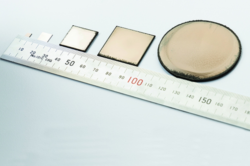
Figure 3. A free-standing diamond substrate with diameter 55 mm.
Over the last three decades there has been an increase in the available substrate sizes of common wide bandgap materials. We have set ourselves the goals of producing a 4-inch diamond substrate in 2025 and an 8-inch one in 2030. In parallel with this increase in diameter, there must be a reduction in cost if the diamond substrate is to become widespread.
High production costs are mainly due to the expense that’s associated with polishing diamond, which is an extremely hard material. While there’s not space to discuss the details of polishing technology, we are confident that there will be advances that trim costs. By 2030, we intend to produce 2-inch diamond substrates with the same level of price as currently available 2-inch GaN substrates.

Figure 4. Transmission electron microscopy image of (001) heteroepitaxial diamond.
Making devices
Working in partnership with researchers at Saga University, Japan, we have fabricated NO2-doped p-channel diamond MOSFETs on a Kenzan Diamond, formed by the growth of (001) diamond on a (110) sapphire substrate misoriented by 5° in the [0001] c-direction. These transistors exhibit a breakdown voltage of 2568 V, the highest value for a diamond MOSFET (see Figure 6, which includes details of device fabrication). We have also evaluated DC output characteristics, recording a maximum drain current of -0.68 A/mm and an on-resistance of 7.54 mΩ cm2. The maximum experimental Baliga Figure of Merit of 874.6 MW cm-2 was demonstrated. We have our sights set on breaking the record for a GaN device of 2093 MW cm-2.
We have also investigated opportunities for our technology to be applied to the detection of radiation. Already on the market are conventional diamond radiation detectors, made from either very high-quality natural diamond or CVD homoepitaxially grown diamond. Both provide high performance, thanks to diamond’s extreme radiation hardness and its excellent thermal conductivity. However, widespread commercialisation is hampered by size limitations. The introduction of Kenzan Diamond promises to overcome this, thereby diversifying diamond’s applications.

Figure 5.For all wide bandgap semiconductors, substrate size has increased over time.
Through a collaboration with Saga and Tohoku Universities, Japan, we have built a radiation detector that incorporates Kenzan Diamond. The nitrogen concentration in the substrate is below 3 parts per billion, in order to prevent carrier trapping. Characterisation of the device’s capacity for radiation detection involved the use of three different sources: 60Co (1.17 and 1.33 MeV), 137Cs (662 keV), and 133Ba (356 keV). We recorded the output voltage associated with the electron and hole charges induced by radiation, and plotted of the energy spectrum for the three different types of γ radiation source (see Figure 7). Based on these results, it is clear to see that Kenzan Diamond can be used to discriminate between nuclides. This is an encouraging result for developing applications for diamond.

Figure 6. (a) DC output characteristics and (b) maximum off-state
breakdown voltage characteristics of a diamond MOSFET with a gate length
of 2.4 µm. During the fabrication of this transistor, to perform NO2
p-type doping, the H-terminated diamond substrate was subjected to 2
percent NO2 gas diluted in N2. Ohmic contacts were formed with a 50-nm
thick gold layer. A 16 nm-thick Al2O3 bi-layer was deposited as a gate
insulator layer, which also provided the diamond channel with
passivation. Gold formed the gate.
Established high-power devices are encroaching performance limitations, due to overheating. One promising way forward is to integrate GaN with diamond. It is challenging to realise the epitaxial growth of GaN on diamond, due to mismatches in lattice constants and thermal coefficients of expansion. But progress can be made with a different approach – working with Osaka City University, Japan, we have fabricated a GaN/diamond heterointerface using room-temperature, surface activated bonding. We prepared Kenzan Diamond substrates with variations in bowing, thickness, and surface roughness (see Figure 8 for details), and used surface-activated bonding to successfully adhere them to GaN.

Figure 7. Radiation detection results for 60Co, 137Cs, and 133Ba.
Our development of 2-inch crystalline diamond, and our efforts with others at demonstrating devices that incorporate this material, are showcasing its great promise. While there’s still a long way to go, there’s good reason to believe that in time, the world will benefit from the deployment of the ultimate semiconductor.
Figure 8. Surface morphology of Kenzan Diamond for surface-activated bonding, as revealed by (a) laser interferometer and (b) atomic force microscopy. Interferometry reveals bowing below 2 µm and a thickness variation, based on 5 points, of less than 2 µm. According to atomic force microscopy, surface roughness is below 0.1 nm.
Further reading
S.W. Kim et al. Appl. Phys. Express. 14 115501 (2021)
S.W. Kim et al. Appl. Phys. Lett. 117 202102 (2020)


