
Researchers pioneer process to stack micro-LEDs
Georgia Tech and MIT team uses 2D boron nitride and graphene to achieve array density of 5,100 pixels per inch
Researchers from the Georgia Institute of Technology and Massachusetts Institute of Technology (MIT) have developed a new process based on 2D materials to create LED displays with smaller and thinner pixels. Enabled by two-dimensional, materials-based layer transfer technology, the innovation promises a future of clearer and more realistic LED displays.
The team published a paper in the journal Nature in February titled, 'Vertical full-colour micro-LEDs via 2D materials-based layer transfer'. Co-authors also include researchers from Sejong University in Korea, and from additional institutions in the US and South Korea.
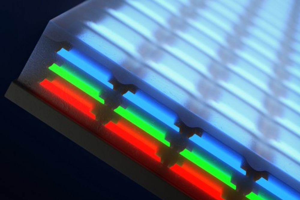
Abdallah Ougazzaden and research scientist Suresh Sundaram (who both also hold appointments in Georgia Tech’s School of Electrical and Computer Engineering) collaborated with researchers from MIT. Instead of using prevailing processes based on laying red, green, and blue (RGB) LEDs side by side, which limits pixel density, the team vertically stacked freestanding, ultrathin RGB LED membranes, achieving an array density of 5,100 pixels per inch — the smallest pixel size reported to date (4 microns) and the smallest-ever stack height — all while delivering a full commercial range of colours.
This ultra-small vertical stack was achieved via the technology of van der Waals epitaxy on 2D boron nitride developed at the Georgia Tech-Europe lab and the technology of remote epitaxy on graphene developed at MIT.
The study showed that the world’s thinnest and smallest pixeled displays can be enabled by an active layer separation technology using 2D materials such as graphene and boron to enable high array density micro-LEDs resulting in full-colour realisation of micro-LED displays.
One unique facet of the two-dimensional, material-based layer transfer (2DLT) technique is that it allows the reuse of epitaxial wafers. Reusing this costly substrate could significantly lower the cost for manufacturing smaller, thinner, and more realistic displays.
“We have now demonstrated that this advanced 2D, materials-based growth and transfer technology can surpass conventional growth and transfer technology in specific domains, such as in virtual and augmented reality displays,” said Ougazzaden, the lead researcher for the Georgia Tech team.
These techniques were developed in MOCVD reactors. The 2DLT technique can be replicated on an industrial scale with high throughput yield. The technology has the potential to bring the field of virtual and augmented reality to the next level, enabling the next generation of immersive, realistic micro-LED displays.
“This emerging technology has a tremendous potential for flexible electronics and the heterogenous integration in opto-electronics, which we believe will develop new functionalities and attract industry to develop commercial products from smartphone screens to medical devices,” Ougazzaden said.


