
NREL team finds unexpected crystal structure in CdTe
Path to better solar cells could yield benefits in catalytic materials, microelectronics, and detectors
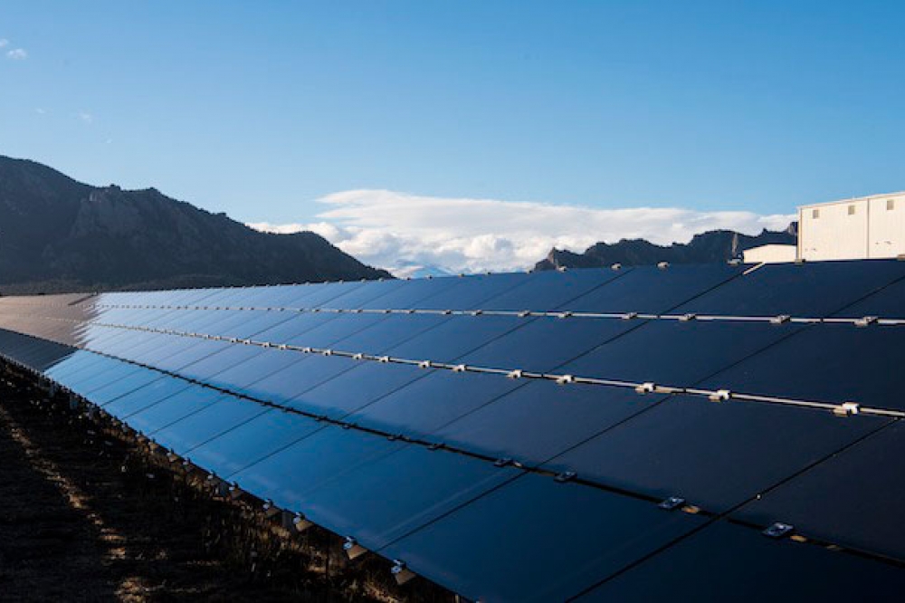
CdTe solar cells are the second-most common PV technology after silicon solar cells. In 2022, they represented about one-third of the US utility-scale solar market.
For more than three decades, PV researchers have known that adding cadmium chloride creates better-performing cadmium CdTe solar cells. But they have not understood exactly why.
A new approach from a team at National Renewable Energy Laboratory (NREL) and colleagues at Khalifa University, Bowling Green State University, and First Solar—an American CdTe solar manufacturer—has unmasked the details of the CdCl2 interface treatment. By modelling the behaviour of individual atoms and electrons, the team simulated possible arrangements for CdCl2-treated interfaces.
In CdTe solar cells, the electrical charges created by an absorbed photon can be trapped and lost at the interfaces between the light-absorbing layer and the layers that carry those charges away into electrical circuits. In the 1980s, CdTe researchers realised that treating the interfaces in the solar cell with a small amount of CdCl2 could reduce the loss of charges at the interfaces and improve the solar cell's power conversion efficiency.
To calculate the electronic structure of a CdTe solar cell - and thereby determine its charge collection— the NREL researchers first needed to determine the atomic arrangement CdCl2 interface, which had never before been done for CdTe solar cells. To achieve this, the team implemented a structure prediction algorithm for interfaces. The algorithm began with a random arrangement of atoms and then allowed them to settle, using a method called density functional theory to calculate the atomic forces. The algorithm repeatedly made small but realistic changes to the positions of the atoms at the interface, which allowed the team to identify the lowest-energy (most stable) structures.
The researchers determined the most stable arrangement of cadmium and chlorine atoms at the interface of tin oxide (SnO2) and CdTe crystals through a structure prediction algorithm. The algorithm generated initial random arrangements of atoms at the interface (left), then updated those arrangements many times and allowed them to relax to their most stable arrangement (right). This revealed that CdCl2 in the interface assumes a unique arrangement not found in larger crystals of the material. This interface-specific atomic structure explains how the CdCl2 treatment improves the performance of CdTe solar cells.
"What surprised us was that the CdCl2 that formed at the interface took a different structure than it would as a bulk material," said Stephan Lany, an NREL computational materials scientist and author on the paper. "It forms a 2D structure that matches both sides of the interface, with boundary conditions different from those when it forms on its own. This means that materials and structures that we don't know or expect might exist for other interfaces as well."
The findings, published in Applied Physics Review, explain how the CdCl2 treatment yields higher-performing CdTe solar cells. By smoothly connecting to the crystal structure on either side of the interface, CdCl2 reduces the defects in the crystal structure that trap charges and reduce solar cell output. Such understanding should aid further improvements to CdTe solar cells.
Broader implications
But Lany and his fellow researchers are most excited by the broader implications of their findings. The CdCl2 structure modelled at the interface does not exist in larger, bulk crystals of the material. The ultrathin interface layer allows a previously unknown form of the material to exist with unique properties. Could this be true for other materials?
"I'm most excited by the realisation that materials do something different when they exist as atomically thin layers on or between other materials than when they are in the bulk," Lany said. "For example, thin functional layers on top of a substrate might assume unique 2D crystal structures with properties different from the bulk material. This might give them new functionalities, for example, in catalysis."
NREL researchers plan to continue to study how materials behave at interfaces. The potential applications stretch beyond photovoltaics, to catalytic materials, microelectronics, electrochemistry (like the water splitting often used to make hydrogen), and detector materials.
"As semiconductor devices increasingly rely on the integration of different materials across interfaces, this enhanced ability to model and tune their structures will allow us to more intentionally design them for better performance," said Kirstin Alberi, director of the Materials Science Center at NREL. "Such insights could open doors for utilising a wider range of materials than previously thought practical."
The research was funded by the US Department of Energy Solar Energy Technologies Office.


