
Perovskite cells - a step towards production
Helmholtz-Zentrum Berlin team shows how precursor inks influence the quality of perovskite thin films
Metal halide perovskites solar cells can be produced with coating processes using liquid inks made from precursor materials and various solvents. After coating, the solvents evaporate and the perovskites crystallise to form a more or less homogeneous layer.
Eva Unger's team at Helmholtz-Zentrum Berlin has extensive expertise in solution-based processing methods and is investigating options for upscaling. "Perovskite photovoltaics is the best solution-processable PV technology available," says Eva Unger, "but we are only just beginning to understand how the complex interaction of the solvent components affects the quality of the perovskite layers."
This is because when the halide perovskite layers are coated on large surfaces, unwanted inhomogeneities can occur, for example so-called ribbing structures.
"By varying the viscosity of the ink, such effects can be minimised," says Jinzhao Li, who is doing his PhD with Unger. At BESSY II, he has investigated how different solvent combinations affect the crystallisation of the perovskite films. The best p-i-n-FAPbI3 perovskite solar cells thus achieve a certified efficiency of 22.3 percent on a laboratory scale.
Jinzhao Li also produced mini solar modules (active area of 12.6 cm2) with colleagues from the HySPRINT innovation lab and PVcomB, which achieved efficiencies of around 17 percent.
Carolin Ulbrich's team tested the optimised solar cells at PVcomB’s outdoor test facility for a whole year: In the process, the efficiency remained almost stable in winter and spring, and only dropped in the warmer summer months. "These tests of larger modules under real conditions give us valuable information on degradation mechanisms to then further improve the long-term stability of halide perovskite photovoltaics," says Eva Unger.
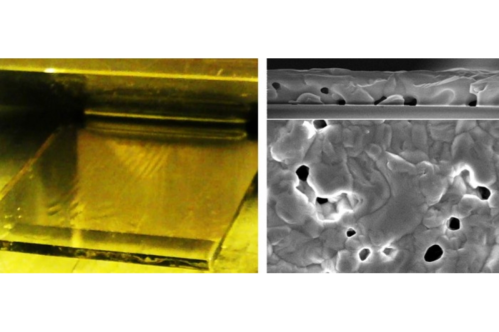
Pictured above: The wet coating with a standard ink composition: the wet perovskite thin films (left) has a rib-like structure. The corresponding SEM image (right) of the annealed perovskite film shows inhomogeneities.
Reference
'Ink Design Enabling Slot-Die Coated Perovskite Solar Cells with >22% Power Conversion Efficiency, Micro-Modules, and 1 Year of Outdoor Performance Evaluation' by Jinzhao Li et al; Advanced Energy Materials (2023)


