
Could OLEDS map magnetic fields?
Australian team shows how a microwave resonator could transform OLED applications
Researchers at the University of New South Wales (UNSW) have demonstrated that OLEDs can be harnessed to map magnetic fields.
The latest research, led by Rugang Geng and Dane McCamey from the UNSW School of Physics, was published in Nature Communications.
“Our findings show that OLEDs, a commercially available technology, can be used not only for displays and lighting, but also for quantum sensing and magnetic field imaging by integrating a small piece of microwave electronics,” says Geng.
“If this technology is properly developed, people could simply use their smartphones to map the magnetic fields around them, for example to spot defects in diamonds or jewellery. This also has applications in industry, such as finding defects in construction materials or as a biomedical sensor.”
How does it work?
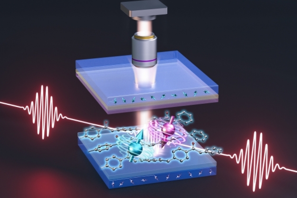
“The basic working principle of an OLED device is that when a voltage is applied, electrons and holes are injected into different layers of the device,” says Geng. “When the electrons and holes meet in the central layer, they form ‘excitons’, which emit visible light when they decay, and that’s what makes OLEDs useful as displays and lighting sources.”
This light emission process exploits the charge characteristics of electrons, which have a negative charge, and holes, which have a positive charge. They both also have another intrinsic property called spin. This spin either points up or down and is very sensitive to external magnetic fields. In fact, it can ‘flip-flop’ (or switch direction) under magnetic resonance conditions.
“By measuring the signal change, both in electric current and emission light, induced by such a flip-flop, we are able to detect the strength of any magnetic field the device is exposed to,” says Geng.
By integrating an OLED with a microwave resonator, Geng, McCamey and their colleagues have generated a tiny oscillating magnetic field across the OLED device, allowing each individual pixel of the OLED screen to act as a small magnetic field sensor.
“We weren’t surprised at the result – we have been pursuing this for a few years,” says McCamey. “But we were surprised at the resolution of the images we could make – we can see details on sub-micron length scales, similar to the size of a bacteria or neuron.”
Commercialisation and everyday uses
Existing quantum sensing and magnetic field imaging equipment tends to be large and expensive, requiring either additional power from a high-powered laser, or extremely low temperatures. Under these conditions, the device integration potential and commercial scalability is limited.
However, the new technique developed by the team can function at a microchip scale and doesn’t require input from a laser, showing great potential for applications in scientific research, industry and medicine.
“Next, we hope to improve the overall performance of the device including optimising the device architecture and exploring other techniques that can significantly increase the field sensitivity,” says Geng.
“We are also exploring collaborations with OLED technology companies as their experience at moving devices from the lab to commercial products will help accelerate translation of this technology.”
Sub-micron spin-based magnetic field imaging with an organic light emitting diode
Reference
'Sub-micron spin-based magnetic field imaging with an organic light emitting diode' by Rugang Geng et al; Nature Communications volume 14, Article number: 1441 (2023)


