
Pioneering N-polar HEMTs
N-polar AlGaN-based HEMTs on AlN substrates offer great promise for excelling in RF performance and thermal management
A US collaboration is claiming to have fabricated the first N-polar GaN/AlGaN/AlN HEMT on a single-crystal AlN substrate.
The team, a partnership between Cornell University, the University of Notre Dame and Asahi Kasei Corporation, says that these transistors have the potential to exploit the thermal and power-handling capabilities of AlN, as well as the merits of N-polar structures, such as a strong back barrier.
Another strength of these HEMTs, which feature AlN buffer layers, is that they don’t require deep-level dopants. In comparison, conventional GaN-based HEMTs need deep-level dopants to compensate for the high unintentional doping concentration in the thick epitaxial GaN buffer layers, which are required to suppress the buffer leakage current and RF loss.
The team’s latest breakthrough, which promises to utilise AlN for high-power, high-frequency and extreme environment applications, builds on its recent success in developing an in-situ cleaning technology for N-polar substrates, which led to the discovery of a two-dimensional electron gas in GaN/Al(Ga)N heterostructure on AlN substrates.
One of the virtues of growth on an AlN substrate is that it ensures a lower dislocation density in the epilayers, typically 104 - 105 cm-2, compared with 109 - 1010 cm-2 for growth on foreign substrates, such as SiC, silicon and sapphire. What’s more, the native substrate removes a high thermal boundary, which has been shown theoretically to overshadow the benefits of a higher thermal conductivity, such as that found in SiC. Commenting on the suitability of their choice of substrate for volume production, spokesman Eungkyun Kim remarks: “Bulk AlN substrates have already demonstrated their high potential as a promising platform for optoelectronics and power/RF devices, and we believe the cost and the availability of AlN substrates will improve as the growth technology becomes more mature.”
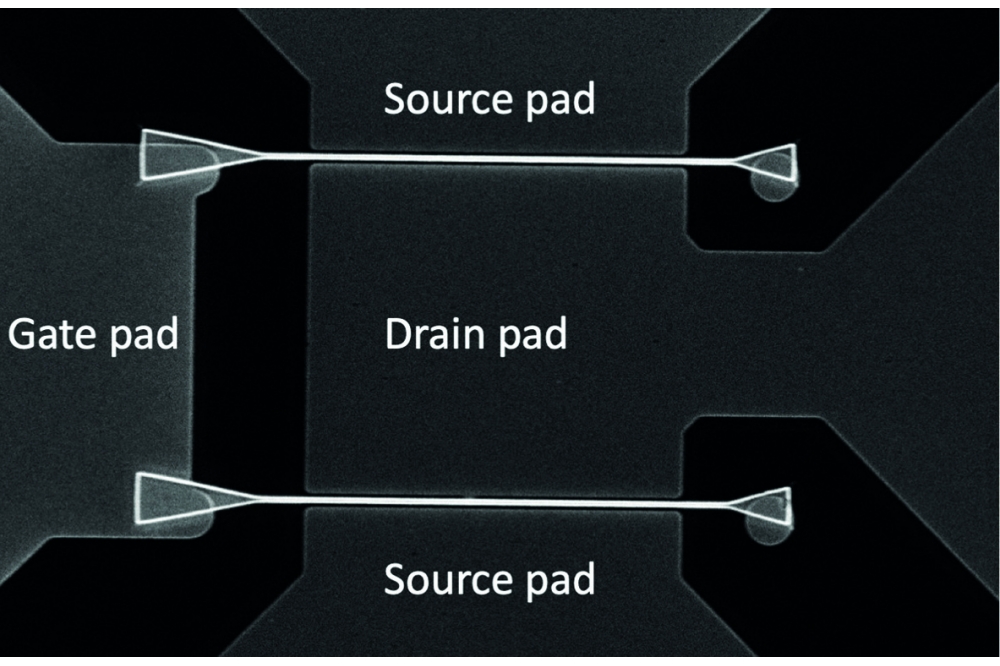
Fabrication of the team’s novel HEMTs began by loading 100 mm-thick Asahi-Kasei N-polar AlN substrates into a plasma-assisted MBE reactor and depositing a 1 µm-thick AlN buffer layer, followed by a 20 nm-thick Al0.91Ga0.09N impurity blocking layer, a 8 nm-thick channel and a heavily-doped 6.4 nm-thick GaN capping layer, employed to enabled easy formation of non-alloyed ohmic contacts. After protecting the N-polar layer by blanket deposition of a 10 nm-thick Al2O3 layer via thermal atomic layer deposition, the team defined source and drain contacts by photolithography, and added a T-shaped gate by electron-beam lithography.
Electrical measurements revealed a contact resistance for the HEMT of 0.66 Ω mm. As there are reports in the literature of a contact resistance of just 0.14 Ω mm for other N-polar HEMTs, the team should be able to trim the contact resistance of its devices.
When moving from a long-channel HEMT to one with a T-gate, on-resistance fell from 4.12 Ω mm to 1.56 Ω mm and maximum drain current increased from 1.2 A/mm to 2.6 A/mm, traits indicative of good scaling behaviour.
Compared with a device with a 500 nm Al-polar AlN layer grown on SiC, the variant on the native substrate had a leakage current through the buffer that’s lower by two orders of magnitude. The team attributes this superiority to the lower dislocation density in the epilayers.
RF measurements revealed a maximum oscillation frequency of 100 GHz and a cut-off frequency of 68 GHz, held back by a high parasitic source resistance and a low transconductance.
Kim admits that many electrical issues need to be addressed with these first-generation devices. “The most important areas to address right now are to achieve a higher transconductance, a lower gate leakage, and a larger breakdown voltage. Once we optimise the electrical properties of our HEMTs, we plan to take a deep dive into thermal properties and show that the heating problem can be solved at a device level by eliminating the thermal boundary resistance at the growth interface.”
Pictured above: A scanning electron microscopy image of a fully processed N-polar HEMT.
Reference
E. Kim et al. Appl. Phys. Lett. 122 092104 (2023)


