
Refining the tunnel-junction in UV LEDs
Tunnel junctions with compositional grading and a high level of doping reduce the voltage drop in UV LEDs
One of the challenges with the UV LED is to develop a design that allows the injection of carriers into the device while avoiding optical absorption and a hike in the operating voltage.
Offering a breakthrough in this regard is a team from The Ohio State University and Sandia National Labs. They meet all these objectives with a AlGaN tunnel junction with compositional grading and a high level of silicon doping.
The external quantum efficiency for these devices is only just over 1 percent, but optimisation of the growth conditions for the active region and the introduction of extraction techniques could lead to higher values, according to team spokesman Agnes Maneesha Dominic Merwin Xavier from The Ohio State University.
The difficulties of carrier injection into UV LEDs are well known. It is challenging to make an ohmic contact to p-AlGaN, and replacing this with p-GaN or an AlGaN-based superlattice leads to absorption and electrical losses, respectively. Adding to the challenge, the acceptor activation energy in AlGaN is high, causing a low hole concentration in the p-type layers.
One way to address these issues is to introduce a tunnel junction. Other teams produce such structures by combining AlGaN with InGaN and GaN interlayers, but this leads to light absorption. Transparent homojunctions can combat this, but have higher voltage losses, compromising efficiency.
Dominic Merwin Xavier and co-workers avoid all these pitfalls with graded tunnel junctions that have an aluminium content of at least Al0.3Ga0.7N. This type of UV LED exhibits a voltage drop of just 1.86 eV across the tunnel junction at a drive current of 20 A cm-2.
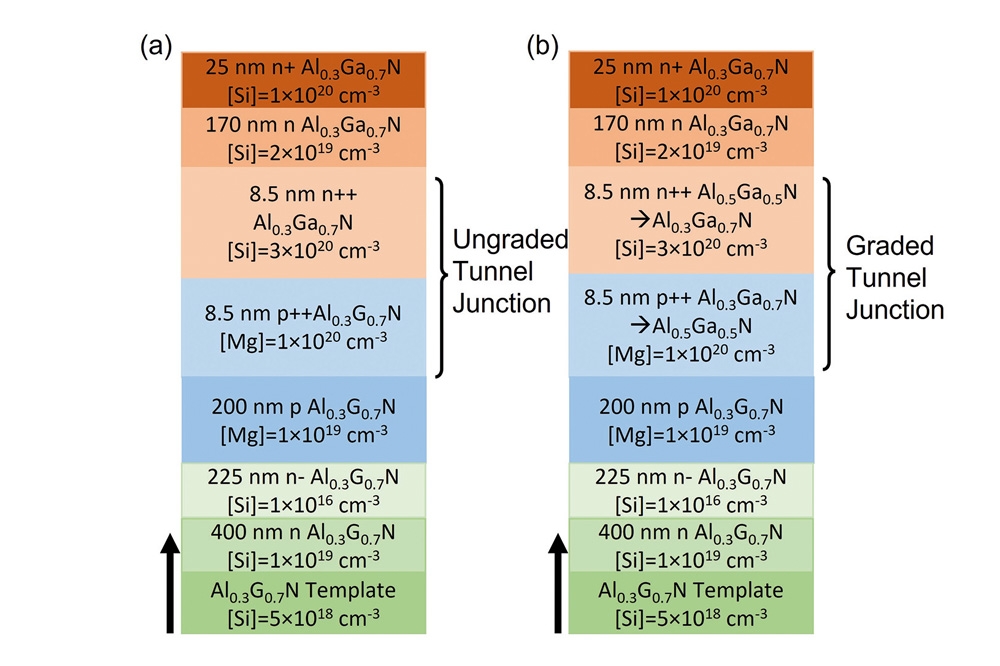
The development of these devices began with a study of the effects of grading in heterostructures featuring a p-n junction and a tunnel junction (see Figure for details of these structures, grown by MBE on MOCVD-grown n-type Al0.3Ga0.7N templates). After etching to define square mesas, the team fabricated devices featuring top and bottom contacts.
Electrical measurements on these structures revealed that grading reduced the total voltage drop across the device at 20 mA cm-2 from 5.26 eV to 5.77 eV.
Modelling with Silvaco Atlas TCD offers some insight into the benefits of grading, including a large concentration of free carriers in the tunnel-junction region, induced by polarisation charges. Compared to a non-graded junction, that of AlGaN with aluminium graded from 30 percent to 50 percent delivered an eight-fold hike in hole concentration and a four-fold increase in the tunnelling rate.
On-wafer measurements of 100 µm by 100 µm LEDs with the graded tunnel junction revealed a voltage drop of 5.55 V. The external quantum efficiency peaked at 1.02 percent for a drive current of 80 A cm-2, and an increase in drive current from 100 A cm-2 to 350 A cm-2 produced a shift in the emission peak from 339 nm to 343 nm.
While MBE has been used to produce these devices, they could also be grown by MOCVD, a technology better suited to mass production.
Dominic Merwin Xavier says that by optimising the doping and grading of the tunnel junction layers, the approach the team has used to make devices emitting above 300 nm could be extended to UVC LEDs, which emit below 280 nm. “However, there may be a higher voltage penalty as the composition of the AlGaN layers increase.”
She says that the next goal for the team is to extend their design and optimise the tunnel junction for low voltage UVC tunnel-junction LEDs.
Pictured above: Comparing electrical characteristics of diodes revealed the benefits of a graded tunnel junction.
Reference
A. M. Dominic Merwin Xavier et al. Appl. Phys. Lett. 122 081108 (2023)


