
CEA-Leti shows that electrons move faster in GeSn
Vertical GeSn transistors could enable low power, high performance chips
CEA-Leti research scientists have demonstrated that electrons and other charge carriers can move faster in germanium tin than in silicon or germanium, enabling lower operation voltages and smaller footprints in vertical than in planar devices.
This proof-of-concept breakthrough means vertical transistors made of GeSe are promising candidates for future low-power, high-performance chips and possibly quantum computers.
GeSe transistors exhibit an electron mobility that is 2.5 times higher than a comparable transistor made of pure germanium. GeSn is otherwise compatible with the existing CMOS process for chip fabrication. Because germanium and tin come from the same periodic table group as silicon, these transistors could be integrated directly into conventional silicon chips with existing production lines.
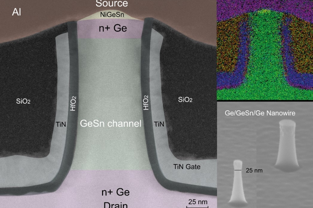
A recently published paper in Nature Communications Engineering, 'Vertical GeSn Nanowire MOSFETs for CMOS Beyond Silicon', notes that “GeSn alloys offer a tunable energy bandgap by varying the Sn content and adjustable band off-sets in epitaxial heterostructures with Ge and SiGe. In fact, a recent report has shown that the use of Ge0.92Sn0.08 as source on top of Ge nanowires (NWs) enhances the p-MOSFET performances.”
“In addition to their unprecedented electro-optical properties, a major advantage of GeSn binaries is also that they can be grown in the same epitaxy reactors as Si and SiGe alloys, enabling an all-group IV optoelectronic semiconductor platform that can be monolithically integrated on Si,” the paper reports.
That project research included contributions from several organisations in addition to CEA-Leti, which delivered the epitaxial stacks. Epitaxy is carried out on a very ordered template, a silicon substrate, with a very precise crystal structure. By changing the material, CEA-Leti duplicated its diamond crystalline structure in the layers it put on top.
“Epitaxy is the art of making multi-layers by duplicating the original structure and is performed at low temperature with gaseous precursors in a chemical vapor deposition (CVD) reactor,” said Jean-Michel Hartmann, a CEA Fellow and team leader, group-IV epitaxy at CEA-Leti.
Depositing this kind of stack and mastering the epitaxial-layer growth is an extremely complex step in a process flow requiring patterned cylinders and conformal gate stack deposition – in short, manufacturing the entire device. CEA-Leti, one of the few RTOs globally that is able to deposit such complex in-situ doped Ge/GeSn stacks, performed that part of the joint research reported in the paper.
“The collaboration demonstrated the potential of low-bandgap GeSn for advanced transistors with interesting electrical properties, such as high carrier mobilities in the channel, low operating voltages and a smaller footprint,” explained Hartmann, a co-author of the paper. “Industrialisation is still far away. We are advancing on the state of the art and showing the potential of germanium tin as a channel material.”
The work also included scientists from ForschungsZentrum Jülich, Germany; the University of Leeds, United Kingdom; IHP- Innovations for High Performance Microelectronics, Frankfurt (Oder), Germany, and RWTH Aachen University, Germany.


