
An easier way to make 2D materials?
Scientists develop simple method to produce large and clean 2D samples from a range of materials
Ever since the discovery of graphene two decades ago, interest in 2D materials has grown. Famously, graphene was produced by exfoliating bulk graphite using sticky tape. While good enough for a Nobel Prize, this method has its drawbacks.
An international team of surface scientists has now developed a simple method to produce large and clean 2D samples from a range of materials using three different substrates. Their method, kinetic in situ single-layer synthesis (KISS) was described in the journal Advanced Science on 1st June in the paper 'In situ exfoliation method of large-area 2D materials'.
There are two ways to produce 2D materials: exfoliating a larger crystal or growing a 2D layer. Exfoliation means peeling off layers from a larger crystal until you are left with just one layer. "This process is time-consuming and requires specific skills and equipment", says Antonija Grubišić-Čabo, a surface scientist at the University of Groningen (the Netherlands) and first author of the Advanced Science paper. "Furthermore, it often results in very small flakes, while the adhesive tape that is used can leave polymers on their surfaces."
Growing 2D films is another approach. This allows the production of large samples under controlled conditions. "However, it often takes a lot of time to work out how to grow such 2D materials. And the process doesn’t always result in a perfect layer," says Grubišić-Čabo. Together with last author Maciej Dendzik, she assembled a ‘dream team’ of colleagues, many of whom had previously worked together at Aarhus University (Denmark) as PhD students, to develop a simple technique for the production of 2D materials.
Their technique uses a gold crystal in a high vacuum chamber. In their first attempt, they "slammed the crystal on bulk material and discovered that a nice 2D layer stuck to the gold.’ Why this happens is not yet clear, but the team suspects that the bond with the gold is stronger than the Van der Waals force that keeps the layers in the bulk crystal together.
They have since built on this first experiment, adding a spring to the stage with the bulk material which acts as a shock absorber and thus allows better control of the impact of the gold crystal.
Furthermore, the team showed that both silver and the semiconductor germanium could be used as a substrate to peel off 2D materials. "Gold crystals are a standard feature in surface science labs, where they are used in the calibration of instruments, for example. Scientists don’t like to damage these crystals, but that didn’t happen in these experiments," says Grubišić-Čabo. "And we have since changed the protocol to use single crystal gold thin films. This has the added advantage of being able to dissolve the gold so that we can isolate the 2D sample, as long as it is stable in air or liquid."
The team has now exfoliated in situ multiple metallic and semiconducting transition metal dichalcogenides onto Au, Ag, and Ge. The exfoliated flakes are found to be of sub-millimeter size with excellent crystallinity and purity, as supported by angle-resolved photoemission spectroscopy, atomic force microscopy, and low-energy electron diffraction.
The approach is said to be well-suited for air-sensitive 2D materials, enabling the study of a new suite of electronic properties. In addition, the exfoliation of surface alloys and the possibility of controlling the substrate-2D material twist angle is demonstrated.
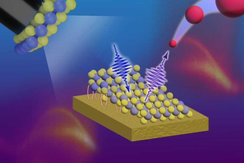
Pictured above: An artistic depiction of the exfoliation and photoemission experiment. 2D material is separated from the parent crystal due to stronger interaction with the substrate. UV light is used to photo-emit electrons allowing studies of the electronic structure by direct imaging of the electronic bands, as seen in the background.


