CS Mantech: Evaluating the pros and cons of power GaN

Switching to a vertical architecture addresses concerns associated with on-resistance and capacitance, but the choice of substrate involves compromise.
BY RICHARD STEVENSON, EDITOR, CS MAGAZINE
The outlook for the GaN power device is incredibly positive. Spurred on by ramping revenues for power supplies in the consumer, telecom and datacom sectors, sales are sure to rocket over the next few years. According to the French market analyst Yole Intelligence, total revenue is going to eclipse $2 billion by 2027 – that’s massive growth, considering sales in 2021 were worth just £126 million.
Yet despite all this success, GaN power devices are far from perfect. The harsh reality is that there are many opportunities for improvement. And while some progress might be baked into the upbeat forecast by Yole, it is clear that the more that’s done to eradicate weaknesses, the better the long-term prospects for this class of power electronics.
At this year’s CS Mantech, held in Orlando, Florida, in mid-May, the most noteworthy weaknesses of the GaN power device were discussed in detail by Mariko Takayanagi, a Senior Manager from Toshiba Electronic Device and Storage Corporation. Several speakers that followed Takayanagi discussed switching to a vertical architecture, which is one option for addressing some of the weaknesses of the traditional power device. Those pursuing a vertical architecture include: Travis Anderson, from the US Naval Research Lab, who detailed the scalable manufacture of planar and vertical p-i-n diodes; Dinesh Ramanathan from NexGen Power Systems, who outlined what is claimed to be the world’s first commercially available GaN-on-GaN technology; and Eldad Bahat Treidel from FBH, Berlin, who described efforts to develop and characterise high-quality drift regions in vertical devices.
Figure 1. The architecture (top) and an optical image (bottom) of the
vertical p-i-n diodes developed at the Naval Research Laboratory, in
collaboration with researchers at Vanderbilt University and Sandia
National Labs.
Lateral limitations
Takayanagi, who works for one of the largest and most established makers of power devices in the world, pointed out that according to market forecasts, for the next few years sales of SiC devices will be worth far more than those for GaN, despite the latter having superior potential, based on Baliga’s figure of merit. The reason for this, argues Takayanagi, is that circuit designers cannot simply swap a silicon power device for one made from GaN.
Two of the great strengths of GaN are its very high values for mobility and saturation velocity. Together, they ensure that devices made from this material switch at frequencies that are more than an order of magnitude higher than those of silicon incumbents. Switching at far higher frequencies is a very valuable asset, because it tends to enable the introduction of far smaller passive components, particularly inductors and transformers. In turn, this enables a trimming of the size of electrical units. What’s more, reverse recovery losses are close to zero, thanks to the non-existence of an anti-parallel body diode. This ensures that a low switching loss is even sustained at high frequencies.
The upshot of all these merits is the possibility to produce power-conversion equipment that is relatively small, while operating at very high power densities and efficiencies. All these strengths are valued by the designers of AC adaptors, micro-invertors, server power supplies and 5G/6G base stations.
Unfortunately, increasing the switching frequency with the introduction of GaN devices can bring its own problems. When moving to megahertz switching, electromagnetic noise may arise in regulated frequency domains. Rules are in place for good reason, as noise suppression is needed to avoid the erroneous turn-on of GaN power devices – if this were to happen, it could lead to a ground fault in power electronic equipment.
According to Takayanagi, the solution to combining a high efficiency at a high switching frequency with low noise generation is to minimise parasitic inductances and capacitances. This can be realised by placing the gate drive and the GaN power semiconductors as close to one another as possible, while minimising the parasitic inductances between the device terminals of a discrete power device.
It is a requirement that is included in what Takayanagi considers to be the three key criteria for the GaN power device, judged from an application viewpoint. These three pillars are: the need for a low on-resistance and parasitic capacitance, to ensure good switching characteristics, low energy loss and low noise; a threshold voltage that’s above around 2.5 V, so that the device is immune to noise and will provide fail-safe operation; and a low overall cost.
The three classes of GaN power devices on the market today are different forms of HEMT. There is the normally-on transistor, which may also be described as a depletion-mode device; the normally-off transistor, also known as an enhancement-mode device; and the cascode variant. Takayanagi has evaluated the pros and cons of these three designs of HEMT.
Figure 2. Vertical p-i-n diodes under forward and reverse bias have
uniform turn-on characteristics, but a very broad distribution in
breakdown behaviour.
Merits of the normally-on transistor, which is on when the gate is biased to zero, include a very high mobility and a zero reverse recovery capacitance, traits that are preferable for high-frequency switching. However, this class of HEMT has a threshold voltage around -10 V, with less than -15 V required to ensure turn off. According to Takayanagi, having the device on at zero gate bias is fatal for power conversion applications, as it requires engineers to put great effort into designing circuitry and gate control, to ultimately ensure safety. The additional circuitry increases parasitics and costs. Due to this, normally on HEMTs are unable to provide high efficiency, high power density and low noise.
Introduced to address issues surrounding the normally-on HEMT is the variant with a cascode configuration. In this case, the normally-on HEMT is connected in series to a silicon low-voltage MOSFET – the source terminal of the MOSFET is connected to the gate terminal of the normally-on HEMT. As a commercial gate driver may be used, there are no concerns relating to cost. But there are concerns associated with the reverse recovery capacitance and the additional on-resistance of the low-voltage MOSFET. It’s possible to address these weaknesses by changing the configuration of the MOSFET and HEMT, but that introduces special drivers, additional components, a power supply and the need for sophisticated control. The third class of commercial HEMT, which is described as normally-off, promises to be the ultimate solution to all three of Takayanagi’s criteria. This mode of operation may be realised with a p-GaN gate, which is unfortunately sensitive to over-voltage. Addressing this particular weakness is the commercially available hybrid-drain embedded gate injection transistor, which maintains zero recovery capacitance and is blessed with an on-resistance that is considerably lower than that of cascode devices. However, the threshold voltage is less than +2 V, which is just shy of what a power electronic engineer desires, according to Takayanagi. This means that there is the threat of erroneous turn-on. Additional concerns are the need for a dedicated driver to provide a current source, and some reliability issues, such as instability due to trapped charges.
To enable GaN transistors to fulfil their potential, demonstrated by their excellent value for the Baliga figure of merit, Takayanagi suggests a need to switch to a different device architecture that combines a high threshold voltage with a low on-resistance and a low capacitance.
Offering promise on all these fronts are vertical GaN transistors. Ideally they are grown on a native foundation, as they require thick drift layers, so demand lattice matching of the substrate and epistructure.
Figure 3. The reverse bias of a FBH Berlin p-n diode with a drift region doped to 4 x 1016 cm-3 shows avalanche behaviour.
Pilot production
In the US, a collaboration that’s led by the US Naval Research Laboratory and includes researchers at Vanderbilt University and Sandia National Labs, has established a pilot production line for producing vertical GaN diodes. A major motivation for this work is to address significant challenges that are holding back the mass production and widespread adoption of vertical GaN devices. According to the team, the relationship between substrate specifications and device performance is not well understood, ion implantation technology for selective-area p-type doping is not reliable, and there is a poor understanding of device failure mechanisms, due to a lack of large data sets from electrical stressing.
Efforts by the partnership have focused on a comprehensive study of incoming metrology and wafer mapping. The team has developed a fully planar device process for making diodes, which can be scaled to provide practical voltage and current levels – the target is 10 A and 1.2 kV.
Key accomplishments by the team include establishing pass/fail criteria for incoming epitaxial layers, and identifying the impact of substrate and epiwafer defects on device performance. To succeed in this endeavour, they are producing a large quantity of devices, with more than 500 coming from every wafer. By employing a constant process, the engineers can directly probe the effect of scaling to large-area devices and to layers designed for higher voltage operation, such as 3.3 kV.
The pilot line uses 50 mm free-standing GaN wafers. Spokesman for the team, Travis Anderson from NRL, accepts that this size is not ideal for cost-effective high-volume manufacturing. He told Compound Semiconductor that high volume fab infrastructure available for supporting 50 mm wafers is not really available, and yield suffers when attempting to make devices of practical size – that is, greater than 1 mm2 – due to the limited available area.
“At 100 mm it becomes much more feasible for a true production environment,” added Anderson. “However, 50 mm is more than sufficient for a manufacturing demonstration to evaluate process stability in an R&D environment, which was the goal of our efforts.”
The winner of this year’s CS Mantech 2023 Best Student Paper Award went
to Yulin He for her paper Hybrid Etching Process on Type-II GaAsSb/InP
DHBT for 5G and Millimetre-Wave Power Amplification.
There are concerns related to the cost, size and level of availability of GaN substrates. “I do not think the cost is prohibitive, particularly as 100 mm wafers are emerging,” argues Anderson, who says that over the course of his collaboration’s four-year programme, they have seen a significant shift in the economics of GaN wafers. “Even though the price has only modestly decreased, the quality and uniformity of the wafer has improved substantially, which improves our process yield.” During the project, the team had no difficulty securing wafers from multiple sources. However, it should be noted that the total number of wafers they have used is not that high.
Anderson and his co-workers used their line to produce 1.2 kV diodes with an 8 µm-thick drift layer doped to 1 x 1016 cm-3, and 3.3 kV variants with a 25 µm-thick drift layer doped to 4 x 1015 cm-3. These devices featured an anode with dimensions varying from 300 nm to 500 nm, and a doping level from 3 x 1017 cm-3 to 2 x 1019 cm-3.
“The p-i-n diode is an ideal test vehicle to understand the fundamentals of a GaN p-n junction,” says Anderson. “Since the p-n junction is the building block of more complicated diodes and FETs, we chose to study the p-i-n diode first as a test vehicle to prove that we can reliability make high quality p-n junctions, evaluate edge termination processes, and study scaling to high current before moving to more complex three-terminal structures.”
The metrology applied to the incoming wafers includes: C-V mapping with a mercury probe, to calculate doping and uniformity; optical profilometry; and X-ray diffraction mapping. The optical profilometry data is analysed with a machine learning algorithm that identifies bumps, pits, and regions of high roughness.
Anderson says that machine learning has been extremely helpful: “As we worked through the fabrication process, we used machine learning to correlate incoming metrology data to device performance data. By working with these data sets, we were able to develop algorithms to develop the appropriate incoming wafer and epi requirements, screen out wafers that would not yield well, and identify non-intuitive mechanisms that would impact device performance.”
Following metrology, wafers are cleaned, before edge termination is realised using a multi-step nitrogen implant box file. This step isolates devices through the p-GaN layer and forms an edge termination region that utilises the hybrid structure, which consists of a junction termination extension region, with guard regions superimposed via a spacer layer (see Figure 1). After cleaning, a front side p-ohmic metal contact and a backside n-ohmic metal contact are deposited.
Electrical measurements under forward bias have produced varied results. On an exceptional wafer, diodes have a highly uniform turn on, a low leakage and high current capability (see Figure 2 (a)). This is said to be indicative of a high-quality p-n junction and relatively few pinholes in the film. However, on inferior wafers many devices suffer from premature turn-on, due to shorting of the anode metal to the substrate. This is caused by pinholes in the epitaxial layer, due to particles introduced in the growth process.
Anderson and co-workers find a very broad distribution in the breakdown behaviour of their diodes (see Figure 2 (b)). For the best discrete devices, breakdown is 1.4 kV, with a leakage below 1 nA at up to 1 kV. But there are also many devices with a high leakage at a voltage just half that of breakdown.
The team are yet to determine the mechanism behind the wide variation in breakdown behaviour. However, they speculate that it could come from localised variations in drift layer properties, arising from variations in miscut or epitaxial defects.
Efforts have been directed at optimising the edge termination design, critical to realising an abrupt avalanche breakdown. The team varied the anode thickness, which ensured a systematic variation in the thickness of the remaining p-GaN layer. This led them to discover that they could slash the leakage current under reverse bias by more than two orders of magnitude by thinning the underlying p-GaN layer to less than 10 nm.
Encouragingly, the team can report two observations that are consistent with avalanche breakdown. One is an increase in the breakdown voltage at elevated temperature; and the other is the moving of an electroluminescence spot from the edge of the isolation implant to the edge of the anode.
Anderson and his colleagues noted a substantial variation in diode performance from wafer-to-wafer. This is attributed to either variations in the epitaxial layers, such as drift layer doping or anode doping, or to differences in the back side of the wafer.
The team have also investigated packaged devices, developing a surface mount process using a commercially available package and outsourced mounting and wire bonding. Following packaging, devices are encapsulated with Hysol. This led to improved performance and no device degradation, benefits that are attributed to passivation.
Having completed fabrication of many devices, one of the plans for the team is to work with circuit designers to evaluate devices in practical applications.
“I am also interested in probing device reliability to understand failure mechanisms,” adds Anderson. “Finally, I see large-area devices as a challenge and am interested in continuing to scale device size.”
Figure 4. The reverse bias of a FBH Berlin p-n diode with a drift region doped to 4 x 1016 cm-3 shows avalanche behaviour.
Commercialising GaN-on-GaN
Details of what is claimed to be the world’s first commercial GaN-on-GaN power technology were described by co-founder of NexGen Power Systems, Dinesh Ramanathan. This Californian outfit, which is now sampling 700 V and 1200 V enhancement-mode JFETs – full production is slated for later this year – boasts that its devices have a superior breakdown voltage and current capability for a given chip area up to 4 kV, compared with any other GaN device, as well as low capacitance and switching losses. Other attributes are said to include: repeated cycle avalanche robustness, thanks in part to the p-n junction; a best-in-class temperature coefficient; and the smallest size, compared with other power semiconductors, for a given current rating.
Ramanathan discussed solutions to many of the challenges associated with the manufacture of GaN-on-GaN devices. To enable high-volume manufacturing, NexGen employs widely available manufacturing tools, modified to handle the transparent, fragile GaN substrates. The company is working with substrate vendors to improve substrate characteristics, such as surface finish, flatness and the level of macro-defects. In addition, efforts are directed at improving NexGen’s epitaxial process, as well as etching and cleaning techniques that can aid the quality of the regrown junction, and the development of novel test structures to improve quality control.
Developing drift regions
A key element in vertical power devices is the drift layer. Evaluating its characteristics using a full device structure is a time-consuming process, so to speed this assessment a team from FBH, Berlin, have been developing approaches based on the use of process control measurement (PCM) structures.
At last year’s CS Mantech FBH’s Eldad Bahat Treidel outlined a PCM structure for measuring the drift region conductivity, and at this year’s meeting he detailed further progress – values for the blocking strength are now possible.
Treidel told Compound Semiconductor that the time it takes to produce a PCM structure is just a third of what it would take to fabricate a complete transistor. What’s more, it is simpler and cheaper. “For example, process and full wafer characterisation of a PCM structure would require 6 lithographic layers as compared to a full transistor process with 12 to 15 lithographic layers.”
In the work described in Orlando this May, Treidel produced p-n diodes that target avalanche behaviour, which is a desirable attribute, as it combines the maximum blocking in the drift region with the highest conductivity.
“In addition, avalanche breakdown is controllable, repeatable, can be predicted and it’s nondestructive and recoverable,” adds Treidel, who points out that these strengths enable a significant reduction in the device design margin between the rated voltage and the real breakdown voltage. “Further, [avalanche] improves short-circuit robustness and ruggedness.”
The team produced its p-n diodes on sapphire substrates. They have been developing vertical GaN-based power devices on foreign substrates, such as sapphire and silicon, through a Europen project called YESvGaN. As well as issues associated with wafer bow, substrate removal and processing of membranes, they have had to consider the high defect density in the drift layers that threatens to limit the blocking strength, reduce the conductivity of the drift layer and impact channel inversion.
None of these issues have proved showstoppers for Treidel and his colleagues. “In the frame of this project we have demonstrated high-quality epitaxial layers with avalanche capability and low resistivity for both GaN-on-sapphire and GaN-on-silicon.”
Figure 5. For p-n diodes with a drift region doped to 3.5 x 1016 cm-3, plots of reverse bias reveal a hard breakdown.
The engineers at FBH fabricated diodes from five GaN epistructures with drift regions with different doping concentrations, all grown on 100 mm sapphire substrates. All these variants, grown by MOCVD, had epitaxial stacks consisting of a 2.2 µm-thick unintentionally doped GaN buffer layer, a 2.4 µm-thick highly conductive drain layer, and a 5 µm-thick drift layer. After determining the doping concentration of the drift layer by electrochemical capacitance-voltage measurements, these structure were loaded into another MOCVD reactor, where a 500 nm-thick layer of magnesium doped at a concentration of 1 x 1019 cm-3 was added, followed by a 30 nm-thick layer of GaN doped to 2 x 1019 cm-3, prior to in-situ activation. Quasi-vertical p-n diodes were formed from these epiwafers by first applying rapid thermal annealing to remove hydrogen from the p-type layers, before using optical lithography and etching to define mesa structures. Ohmic p-type and n-type contacts were then formed, before the passivation of the mesa edges via plasm-enhanced CVD added 200 nm of SiN (see Figure 3).
Electrical measurements on all the devices determine that it is just the variant with the highest doing in the drift region – it’s doped to 4 x 1016 cm-3 – that exhibits avalanche behaviour (see Figure 4). The other four, with doping in the drift region varying from 3.5 x 1016 cm-3 to 3.5 x 1015 cm-3, undergo a non-avalanche hard breakdown (see Figure 5). According to the team, these findings indicate that as the concentration of doping in the drift region reduces, there is a shift from the parallel plane junction (avalanche) regime to the punch-through breakdown limit.
Triedel and co-workers have benchmarked their devices against other p-n diodes on GaN and sapphire substrates (see Figure 6). It is claimed that the device with a 1.2 x 1016 cm-3 level of doping in the drift region offers excellent blocking performance, with a hard breakdown of 920 V, a drift region specific resistance of 0.57 Ω cm2, and a power figure of merit of 1.43 GW cm-2.
One of the team’s next targets is to develop the growth of GaN layers that are as thick as around 15 µm on sapphire substrates, because this will enable devices to block more than 1.5 kV while exhibiting a specific resistivity of around 1 mΩ cm2. “For this we have developed a strategy to reduce the internal built-in strain in the substrate, and by that to reduce the wafer bow,” says Treidel.
Figure 6. The p-n diodes fabricated at FBH, Berlin, deliver an
impressive performance for variants that have a sapphire foundation.
In parallel, those at FBH will be developing a number of gate module technologies, such as trench MOSFETs, finFETs and finJFETs. It is possible to integrate these technologies on native and foreign substrates.
“Our device processing activities for vertical GaN devices on native and foreign substrates will enable us to study the impact of GaN layer material quality on device performance and reliability,” adds Treidel. The GaN-on-GaN will also enable the team to investigate the influence of different substrate manufacturing methods, such as HVPE and ammonothermal growth, and compare material supplied by different vendors.
Such efforts will help to advance the capabilities of vertical GaN devices, which offer many advantages over their lateral cousins. Progress on both these fronts may well be discussed at the next CS Mantech, which will take place in Tucson, AZ, from 20-23 May 2024.
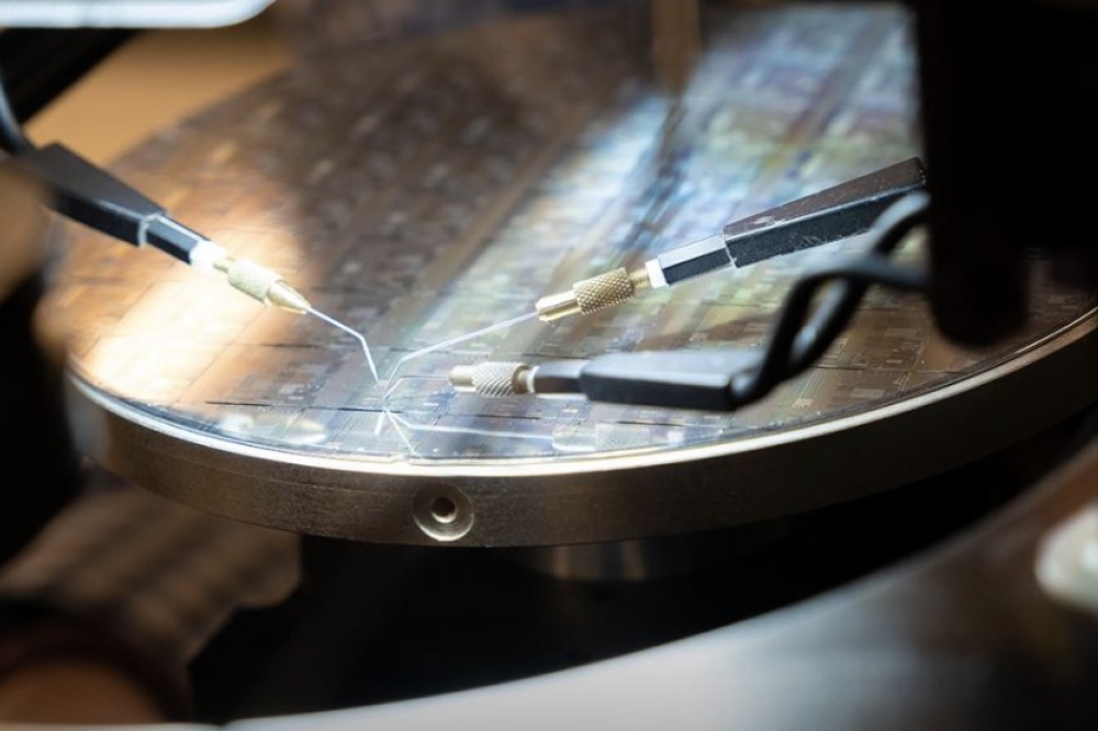
Main image: Bristol University’s Martin Kuball chaired this year’ s CS Mantech. Taking over the reins for 2024 is Peter Ersland from MACOM.


