MBE: A game changer for GaN-on-silicon RF

On the back of remarkable results at 40 GHz, GaN-on-silicon HEMTs have a
tremendous opportunity to serve in mobile applications requiring
high-power millimetre waves.
BY ANDRE BONNARDOT, ELODIE CARNEIRO AND
STEPHANIE RENNESSON FROM EASYGAN AND FABRICE SEMOND FROM UNIVERSITÉ CÔTE
D’AZUR, CNRS-CRHEA
Do you think that GaN-on-silicon will be adopted for RF applications? If you asked that question a couple years ago, the answer could well have been along the lines of a cautious yes, tempered by the point that it’s hard to know when GaN-on-silicon will have an impact, and to what extent. And there was very good reason for this caution: it is challenging to produce GaN-based heterostructures on silicon with sufficient material quality in a reproductible, reliable manner.
Helping spur the development of GaN-on-silicon RF devices are decisions related to the future of the wireless industry. In March 2022, the 3GPP (3rd Generation Partnership Project) standardisation initiative propelled the 5G millimetre wave spectrum limit to 71 GHz, exacerbating the technical challenge for device manufacturers. The reality is that while it is not going to be easy, deploying millimetre-wave bands is inexorable – that’s because higher frequencies are essential for supporting the exponential increase in data traffic created by future 5G advanced networks.
The inevitable march of millimetre-wave standardisation will be challenging for pico-cell and handset vendors. They will be constrained when designing and integrating RF front-ends operating at those frequencies. In turn, this will create a new, high volume, cost sensitive RF device market opportunity for semiconductor manufacturers.
A great candidate for providing the high-power densities at high operating frequencies that’s demanded by this application is the GaN HEMT. The most suitable form of this transistor is the GaN-on-silicon HEMT: it is the technology of choice for GaN electronics, and it is already gaining momentum in power electronics applications.
Today, however, the GaN-on-SiC form of the HEMT is the mainstay in RF applications. Compared with the silicon substrate, SiC provides a superior thermal conductivity as well as more compatible lattice and thermal expansion mismatches (see Table 1). These assets make it easier to produce a device delivering high power at high frequencies. But there are drawbacks, in terms of cost, CMOS compatibility, supply availability and large diameter feasibility. Due to this, there is no question that the GaN-on-silicon HEMT will rise to the fore for high-volume deployment, once technological barriers have been removed.
At EasyGaN, a French start-up founded in 2017 by researchers of CRHEA, a CNRS laboratory that pioneered the field of GaN hetero-epitaxy on the silicon substrate, we are helping to accelerate this switch to GaN-on-silicon. Read on to discover how we are using MBE to transform the capability of this class of GaN HEMT in the millimetre-wave domain.
Figure 1. The original epitaxial structure developed by EasyGaN.
Solving challenges with MBE
The growth of high-quality GaN-on-silicon is a challenge on a number of fronts. The most well-known difficulty comes from the large lattice and thermal expansion coefficient mismatches, which can lead to undesirable defects, such as a high density of threading dislocations and cracks. In addition, the surface of silicon is highly reactive to many chemicals involved in epitaxial growth. The presence of nitrogen leads to nitridation, gallium causes melt-back etching and aluminium diffuses into the highly resistive silicon substrate. Due to all of this, there are unintentional reactions at the interface between the buffer and silicon, as well as inside the silicon sub-surface. The unwanted consequences include parasitic charges, low buffer resistivity and insufficient thermal dissipation. All threaten to hold back the performance of the GaN HEMT – it can be impeded by RF losses, current degradation over time and reliability issues.
Much progress is realised by moving the epitaxial growth technology for GaN-on-silicon from the more common MOCVD to an alternative that is well-established for many III-Vs, MBE. With the latter form of epitaxy, it is possible to obtain very good control of the AlN buffer/silicon substrate interface when using ammonia as the nitrogen source. This success is aided by low-temperature nucleation in an ultra-high-vacuum environment, which eliminates undesired pre-reactions at the surface of the silicon substrate. It is this aspect of growth that enables us to produce AlN buffers on silicon that exhibit unequalled structural quality, uniformity, and smoothness.
Figure 2. Scanning electron microscopy cross-sectional image of an EasyGaN HEMT, showing the ultra-thin hetero-structure.
Back in 2020, using our unique know-how in AlN nucleation on silicon, we started measuring the resistivity of a simple MBE-grown AlN/GaN stack on silicon. Following process tuning, we were able to realise excellent results, including RF losses as low as 0.3 dB/mm at the buffer/substrate interface. Encouraged by this success, we joined the GaNeXT project HUGE, led by Farid Medjdoub from IEMN. This move involved a close collaboration with IEMN and CRHEA, with efforts leading to the fabrication of a complete HEMT structure. Two years in, we obtained remarkable results at the device level.
Through this partnership, our team used a Riber MBE49 reactor with 3 x 4-inch configuration, located at CRHEA, to grow an epi stack on high-resistivity silicon (111) substrates. The resulting epitaxial AlN/GaN heterostructure, grown by ammonia-MBE on 4-inch silicon, features: an AlN nucleation layer; a sub-micron-thick graded and undoped AlGaN buffer, used as a back barrier to enhance both confinement of the 2DEG under a high electric field and the breakdown voltage; and a 150 nm undoped GaN channel material, covered by an ultra-thin AlN barrier (see Figure 1).
Table 1. While there are technical challenges of using substrates made
from silicon rather than SiC for GaN RF devices, there are also
significant economic advantages.
Remarkable results at 40 GHz
Those of you that have been involved with the semiconductor industry for a while will know that development cycle times are very long. That’s at odds with the wishes of a typically stakeholder, and demands a level of patience from them that they are not necessarily used to.
Helping to smooth over the stress at this embryonic time for any fledgling firm is the emergence of some good news from an R&D lab. In our case, this came from unveiling unmatched characteristics for each element of the stack (this is illustrated in Figure 2, which shows a cross-sectional image obtained by a scanning electron microscope).
Figure 3. Secondary ion mass spectrometry reveals low carbon and oxygen
levels in the GaN channel and the step-graded AlGaN buffer layers.
One of the hallmarks of our epistructure, resulting from nucleation of a high-quality AlN layer at a low deposition temperature, is a high resistivity in the thin buffer that limits RF losses in the substrate. Another asset is the low level of impurities in the AlGaN buffer and GaN channel layers that minimises trapping effects (see Figure 3).
Indeed, a significant advantage of using MBE for the growth of aluminium-rich structures is that it enables relatively low levels of carbon and oxygen impurities. For example, we draw on this asset to grow epitaxial HEMT heterostructures with AlGaN channels that enable devices with a high breakdown voltage, a significant merit for power electronics. MBE is also renowned for its abrupt interface control, which ensures a very sharp interface between the barrier and channel, and in turn allows the use of a very thin AlN barrier. Such a barrier is key to doubling the density of the 2DEG, compared with a conventional AlGaN barrier.
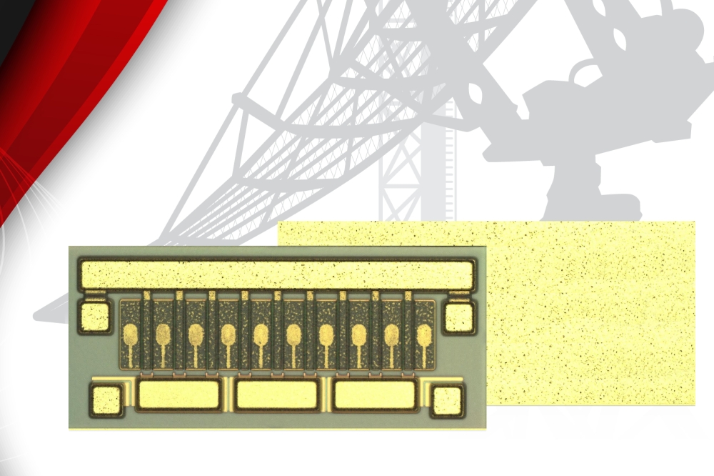
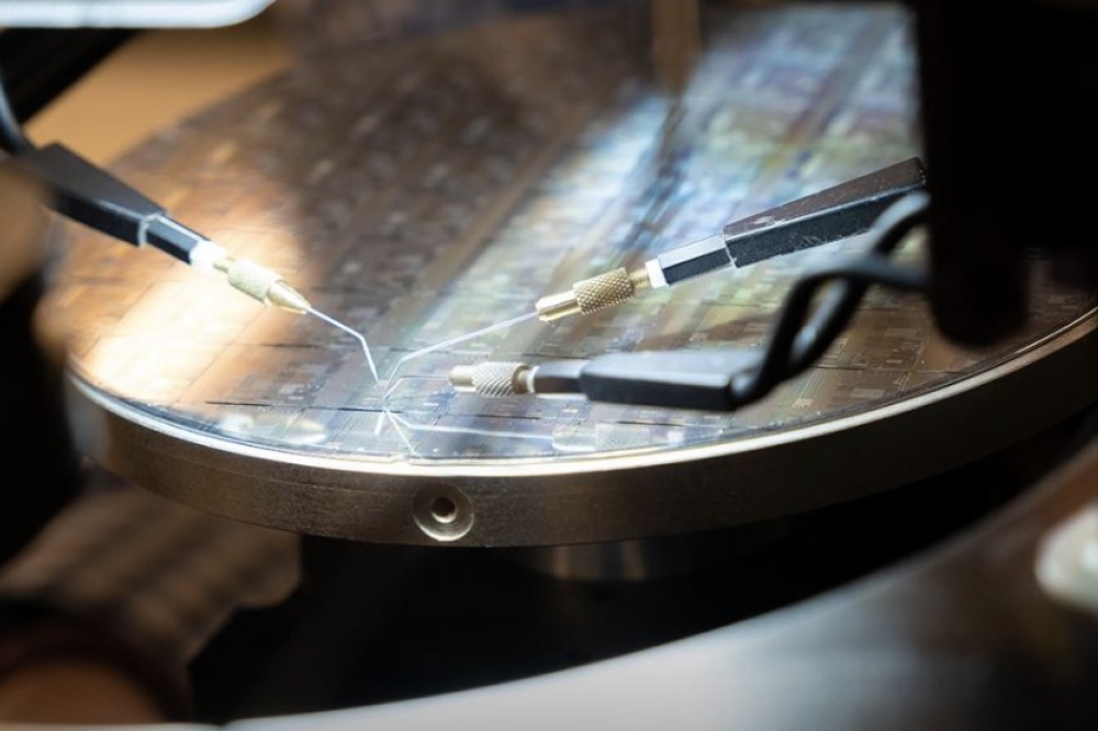
Our team has processed these epiwafers at IEMN, fabricating short transistors that we’ve characterised in a load-pull configuration using a reference 40 GHz power bench (shown in Figure 4). As this bench has also been used to measure state-of-the-art GaN structures on SiC, rigorous benchmarking is assured. Device processing included formation of source and drain ohmic contacts, isolation of devices, defining of T-gates with sub-150 nm lengths by electron-beam lithography, and deposition of a SiN passivation layer.
Figure 4. A processed GaN-on-silicon epiwafer, 40 GHz power test bench at IEMN, and a device under test.
Measurements with the power bench confirmed the excellent robustness of this heterostructure at 40 GHz. It is capable of handling extreme electric fields, and consequently enables high voltage operation without degradation after several tens of load-pull sweeps. Our device delivers 3.5 W/mm, associated with a power-added efficiency of 30 percent at a drain-source voltage of 30 V. That’s a new performance benchmark for this frequency band for the GaN-on-silicon HEMT (see Figure 5).
Figure 5. Values of power-added efficiency versus output power for a
range of GaN HEMTs. More details to be found in the Further Reading
section.
We are also encouraged by our measurements of the maximum frequency (fmax) and the unity gain bandwidth (ft). They show consistent behaviour relative to the gate length of the transistor (see Figure 6). Finally, we recorded a drain leakage current below 10 µA/mm up to a drain-source voltage of 30 V (see Figure 7).
Steps to mass production
To cover the entire range of 5G advanced millimetre-wave bands with some margin, we will now work on extending the operating frequency to 94 GHz.
In addition, we plan to support low-voltage operation, so that our HEMTs can serve in handsets. To meet these goals, we will increase electron mobility, enhance thermal dissipation and trim ohmic contact resistance. For the latter, we are also using MBE, an efficient approach for creating low-temperature highly doped regrown ohmic contacts.
One of our next tasks is to assess the thermal properties of our HEMTs, prior to running our structure through optimisation loops. We are well aware that like any other developer of a GaN-on-silicon device, we are confronted by thermal dissipation characteristics that are poorer than those that come with structures with a SiC foundation. We expect that our sub-micron thick, simple buffer will help to minimise thermal resistance between the active area and the substrate – but we still need to prove this.
Figure 6. Value for fmax and ft as a function of the gate length.
What’s encouraging is that we have margins in our current design that will allow us to compromise between different parameters and tune characteristics to accommodate a wide range of RF GaN applications. One of the beauties of working with the silicon substrate is access to an arsenal of existing sophisticated techniques that will allow us to enhance thermal dissipation in the substrate.
You may wonder why we insist on making our epitaxial structures so thin. The reason is that, as well as the expected thermal benefits that we have already mentioned, thinner layers take less time to grow and lead to a low wafer bow – it is below 20 μm, a great asset when developing larger epiwafers. These strengths translate to a cheaper production cost and a higher yield for device manufacturers, compared with more complex MOCVD-grown structures.
Figure 7. A low value for the drain-induced barrier lowering reflects the excellent electron confinement within the 2EG.
We know that the adoption and deployment of GaN-on-silicon HEMTs produced by MBE will take some time. Establishing the epi design and the recipe is a first necessary step. However, in itself it is not enough. Device manufacturers demand production tools that fulfil cost and throughput requirements found in a high-volume semiconductor market. Whether the MBE systems is the only production tool employed, as is the case with an epiwafer provider, or integrated into a chip fab, key criteria are throughput, cost and yield. Those of us at EasyGaN and CRHEA are well-placed in this regard, as we are already able to manufacture GaN-on-silicon HEMT epistructures on 200 mm wafers in batch mode. For mass production, we can increase scale, moving to Riber’s 300 mm silicon-fab-compatible MBE platform to deliver gains on the capacity and cost roadmap.
With our plans in place to scale manufacture of the GaN-on-silicon HEMT, and results showcasing the prowess of this transistor, it is surely destined for a bright future.
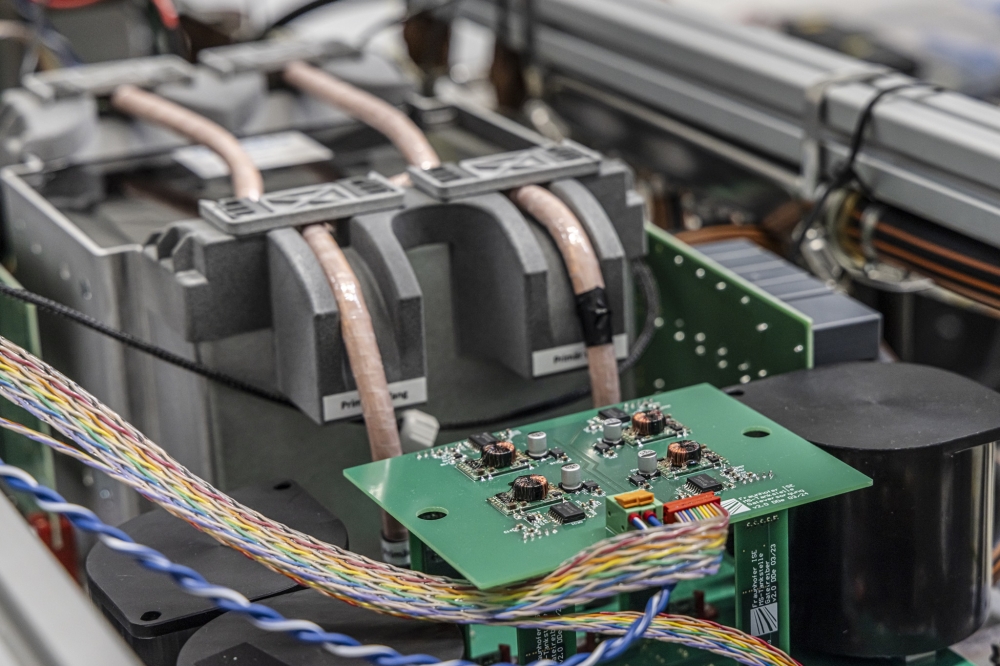
The MBE49 reactor at CRHEA.
Further reading
⬤ E. Carneiro et al. “Sub-Micron thick Step- Graded AlGaN Buffer on Silicon with a High Buffer Breakdown Field” Physica status solidi A 202200846 (2023)
⬤ E. Carneiro et al. “Combination of low trapping effects and high blocking voltage in sub-micron thick AlN/GaN short transistors grown by MBE on silicon substrate Applied Physics Express, submitted (2023)
⬤ R. Kabouche et al. “Power Measurement Setup for On-Wafer Large Signal Characterization Up to Q-Band” IEEE Microw. Wirel. Compon. Lett. 27 419 (2017)
⬤ K. Harrouche et al “Impact of undoped channel thickness and carbon concentration on AlN/GaN-on-SiC HEMT performances” Appl. Phys. Express 15 116504 (2022)


