
InP-based lasers surpass 2.2 µm
Thanks to the antimonide surfactant effect, strained InP lasers are delivering milliwatt emission at almost 2.3 µm
Engineers from NTT, Japan, are claiming to have enhanced the capability of InP-based lasers by smashing through the 2.2 µm barrier. The team’s InP ridge-waveguide lasers, featuring strained InGaAsSb multi-quantum wells, are capable of emitting output powers of several milliwatts at wavelengths up to 2.278 µm.
This breakthrough increases the attractiveness of the InP laser as an alternative to the lattice-matched GaSb-based laser in a number of applications requiring sources in the 2.1 µm to 2.3 µm range. While GaSb-based lasers in this spectral domain can be used for gaseous sensors, biomedical sensors and car exhaust analysers, processing technologies for this material system are not as mature as those for InP, which has been the key material for telecommunications for many decades.
Extending the wavelength of the InP-based laser is far from easy. To reach beyond 2.1 µm with an active region that employs InGaAs quantum wells, strain in this material system must exceed + 1.8 percent. The growth of such structures is challenging, requiring growth temperatures below 500 °C, alongside just a few quantum wells and layers less than 6 nm-thick. Of most concern are defects induced by large strain – they threaten to quash laser emission.
To avoid these issues, the team from NCT has turned to InGaAsSb quantum wells, supressing defect formation with surfactant mediated growth. These engineers are not the first to introduce antimony, which acts as a surfactant during the growth of strained InGaAs wells, but they have stretched the emission further than their peers by cranking up the concentration of this element.
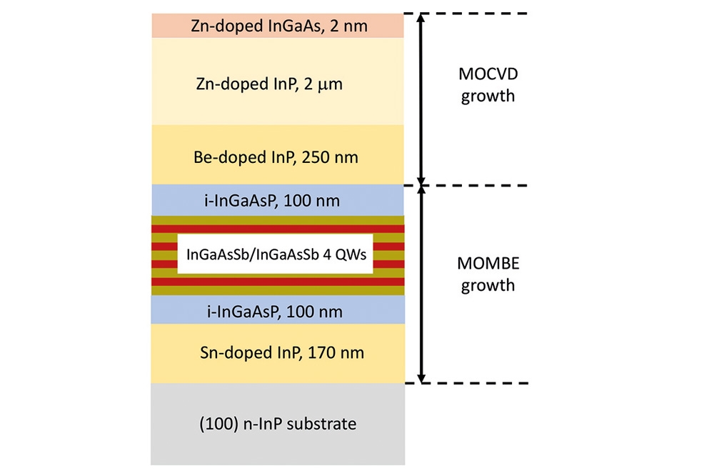
Record-breaking lasers have been realised with a two-step epitaxial process, beginning with the growth of a four-period multi-quantum well active region sandwich by InGaAsP and InP, all grown by metal-organic MBE. After the team studied these structures, they turned to re-growth by MOCVD to add Zn-doped InP and InGaAs layers, prior to the formation of ridge-waveguide lasers. According to team spokesman Manabu Mitsuhara, the strained InGaAsSb lasers produced by NCT, could also be formed by other growth methods, such as MBE and MOCVD, which are capable of growing active regions with sharp interfaces.
Mitsuhara and co-workers studied a pair of samples grown by metal-organic MBE, featuring active regions with different thicknesses. X-ray diffraction determined that both heterostructures have smooth interfaces between the wells and barriers, while simulations of the well-defined satellite peaks suggest that the quantum wells have a strain of +2.3 percent and thicknesses of 6.4 nm in one sample and 8.4 nm in the other. Both samples have 20.6 nm-thick barriers with a strain of -0.23 percent.
Calculations based on the model-solid theory, drawing on photoluminescence measurements and strain value obtained from X-ray diffraction, suggest compositions for the well and barrier of In0.82Ga0.18As0.95Sb0.05 and In0.45Ga0.55As0.95Sb0.05, respectively.
Using standard processes for making InP telecom lasers, Mitsuhara and co-workers have fabricated ridge-waveguide lasers with a cavity length of 600 µm and a stripe width of 2.5 µm. These lasers, with quantum well thicknesses of 6.4 nm and 8.4 nm, produced several Fabry-Perot modes and had peak wavelengths of 2.190 µm and 2.278 µm, respectively, at 15 °C. Driven at 100 mA, the output power per facet of the longer-wavelength source fell from 5.9 mW to 2.4 mW when its operating temperature increased from 15 °C to 55 °C.
Mitsuhara claims that it should be easy to apply their lasers to absorption spectroscopy, which requires a tunable light source with single-mode operation and an output power of several milliwatts.
Reference
M. Mitsuhara et al. App. Phys. Lett 122 141105 (2023)


