
Bifacial perovskite cells show higher efficiency
A bifacial perovskite solar cell, which allows sunlight to reach both sides of the device, holds the potential to produce higher energy yields at lower overall costs, according to scientists at the US Department of Energy’s National Renewable Energy Laboratory (NREL).
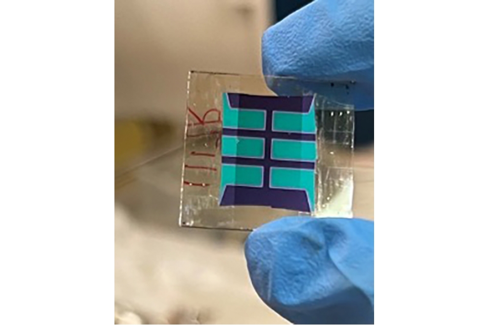
The dual nature of a bifacial solar cell enables the capture of direct sunlight on the front and the capture of reflected sunlight on the back, allowing this type of device to outperform its monofacial counterparts.
“This perovskite cell can operate very effectively from either side,” said Kai Zhu, a senior scientist in the Chemistry and Nanoscience Center at NREL and lead author of a new paper 'Highly efficient bifacial single-junction perovskite solar cells' in published in the journal Joule: His co-authors from NREL are Qi Jiang, Rosemary Bramante, Paul Ndione, Robert Tirawat, and Joseph Berry. Other co-authors are from the University of Toledo.
Past bifacial perovskite solar cell research has yielded devices considered inadequate in comparison to monofacial cells, which have a current record of 26 percent efficiency. Ideally, the NREL researchers noted, a bifacial cell should have a front-side efficiency close to the best-performing monofacial cell and a similar back-side efficiency.
The researchers were able to make a solar cell where the efficiency under illumination from both sides are close together. The lab-measured efficiency of the front illumination reached above 23 percent. From the back illumination, the efficiency was about 91 percent –93 percent of the front.
Before constructing the cell, researchers relied on optical and electrical simulations to determine the necessary thickness. The perovskite layer on the front of the cell had to be sufficiently thick to absorb most of the photons from a certain part of the solar spectrum, but a perovskite layer that is too thick can block the photons. On the back of the cell, the NREL team had to determine the ideal thickness of the rear electrode to minimise resistive loss.
According to Zhu, simulations guided the design of the bifacial cell, and without that assistance the researchers would have had to experimentally produce cell after cell to determine the ideal thickness. They found the ideal thickness for a perovskite layer is around 850 nm.
To evaluate the efficiency gained through bifacial illumination, the researchers placed the cell between two solar simulators. Direct light was aimed at the front side, while the back side received reflected light. The efficiency of the cell climbed as the ratio of reflected light to the front illumination increased.
While researchers estimate that a bifacial perovskite solar module would cost more to manufacture than a monofacial module, over time bifacial modules could end up being better financial investments because they generate 10 percent–20 percent more power.


