Excelling in the etching of gallium oxide
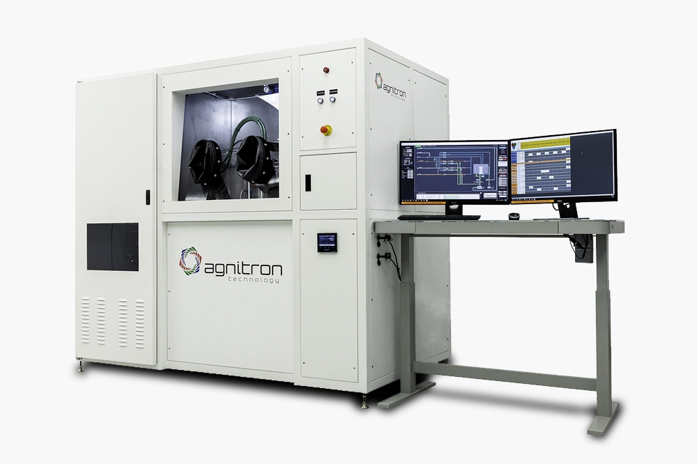
The etching of Ga2O3 works best when using an MOCVD chamber to direct gallium-containing organic molecules onto epilayers.
BY
FIKADU ALEMA, AARON FINE, WILLIAM BRAND AND ANDREI OSINSKY FROM
AGNITRON AND ABISHEK KATTA AND NIDHIN KURIAN KALARICKAL FROM ARIZONA
STATE UNIVERSITY
By taking rapid strides Ga2O3 is now poised to shape the market for power devices. This ultra-wide bandgap semiconductor is equipped with the characteristics to enable superior devices, realised at a very competitive cost, thanks to the opportunity to make high-quality bulk substrates from the melt.
During the last decade, the performance of this class of power device has come on in leaps and bounds. Key breakthroughs have included the fabrication of devices with breakdown voltages of more than 8 kV and breakdown field strengths greater than 5 MV/cm, which is beyond the theoretical limits of SiC and GaN. However, Ga2O3-based devices are yet to produce a level of performance that’s close to the theoretical limit. Why? Well, in part it is due to the lack of appropriate, highly controllable, damage-free etching processes.
Controllable etching and the removal of material are essential steps in the fabrication of many different types of semiconductor devices. The capability to remove material is just as important as the ability to deposit it – this pair of complementary processes enables the shaping of semiconductor materials into well-defined device architectures.
Prior to etching, the active region of many devices tends to be protected by dielectrics, such as SiOx or SiNx. That’s also the case with Ga2O3-based devices. However, it’s not easy to find a damage-free etch process that avoids compromising the performance or the reliability of the device.
A wide range of etch processes have been employed during the fabrication of numerous β-Ga2O3 based devices. These processes include dry etching, wet etching, photochemical etching, and metal-assisted chemical etching. Unfortunately, all these forms of etching exhibit limitations, such as surface damage, the introduction of angled sidewalls, and anisotropic etching along certain crystal planes. Due to these downsides, none of these approaches are suitable for producing high-performance devices.
Offering far more promise are vapour-based in-situ etching techniques undertaken in the chambers of growth tools, such as those used for MBE and MOCVD. By their very nature, such approaches to epitaxial growth enable etching and re-growth of epilayers and dielectrics without breaking the vacuum, resulting in cleaner interfaces. As the quality of β-Ga2O3 epilayers is highest when grown by MOCVD, this type of reactor is the best choice for integrating growth and etching processes.
At Agnitron, we have a well-earned reputation as the leading provider of MOCVD reactors for the growth of β-Ga2O3 epilayers, with our tools now installed in a number of world-class labs. What may be less well known, however, is that our reactors can be used for the in-situ etching of Ga2O3 films, substrates, and related alloys. That’s the topic for the remainder of this article, where we discuss the etching of β-Ga2O3 using metal organic sources containing gallium and chlorine.
Etching with MBE…
The growth of Ga2O3 by MOCVD involves the reaction of gallium and oxygen precursors, with the rate of deposition typically governed by the concentration of gallium that’s introduced into the reactor. However, when the growth chamber is deprived of active oxygen, the gallium precursor performs a different role, etching the surface of the substrate or the epitaxial film.
In MBE, this etching process is well-known. As the growth of Ga2O3 progresses, this competes with the formation of Ga2O3 and its volatile suboxide Ga2O – and when higher gallium fluxes land on the substrate in an oxygen deficient environment, the rate of growth of Ga2O3 decreases (what’s actually happening is that material is etched from the Ga2O3 surface, rather than growing on it).
When these conditions occur, involving oxygen deficiency, they favour formation of the extremely volatile suboxide Ga2O, which desorbs from the surface rather than contributing to the growth of Ga2O3. Due to these conditions, it’s impractical to accelerate the growth rate of Ga2O3 with standard MBE growth processes. Drawing on this phenomenon, many researchers have turned to gallium metal to etch the surface of Ga2O3 in an MBE chamber. According to reports, this is a low-damage etch technique, with gallium reacting with Ga2O3.
....and MOCVD
We have investigated using MOCVD to etch Ga2O3 in collaboration with Nidhin Kalarickal’s group at ASU, who have experience of gallium etching of Ga2O3 in an MBE chamber. Working together, we have shown that in the absence of oxygen, metalorganic gallium-containing precursors, such as triethylgallium (TEGa), enable in-situ etching of Ga2O3 in an MOCVD chamber. Again, etching comes from the reaction of gallium with Ga2O3 to produce the volatile Ga2O suboxide, but this time the process begins with the homogeneous decomposition of TEGa. Pyrolysis takes place when TEGa is exposed to a temperature of around 350 °C or more, which it gets from the substrate temperature, creating gallium adatoms that move over the surface. The stable organic ethylene by-product produced during pyrolysis is removed from the reactor through the exhaust, following minimal interaction with the substrate’s surface.
To monitor the etch rate in-situ, we take advantage of the significant refractive index contrast between the β-Ga2O3 film and the underlying sapphire substrate. We measure the etch rate by installing a fibreoptic reflectometer, operating at 470 nm, in our Agilis 100.
Figure 1. An Agnitron MOCVD reactor with a blue LED shining at the
center of a 2-inch wafer (left). (Right) The red trace is the measured
reflectance data, and the blue trace fits the reflectance data from
which the etch rate is estimated. An etch rate of 9 µm/hr is estimated.
With this set-up, we have investigated the effect of various process conditions on the etch rate of (2.01) oriented β-Ga2O3 epitaxial films grown on c-plane sapphire. In particular, we have studied the TEGa molar flow rate, substrate temperature, and chamber pressure. These experiments reveal that we can vary the etch rate from around 0.3 µm/hr to 9 µm/hr (see Figure 2).
We have found that for low TEGa molar flow rates – that is, values below 100 µmol/min – the etch rate increases linearly with increasing flow rate (see Figure 2(a)). However, at higher flow rates, the etching rate only increases slightly before saturating. When the etching conditions are in the linear regime, the suboxide reaction rate is high enough to consume all the gallium adatoms that are supplied from reaching the substrate surface. Due to this, the etch rate is limited by the supplied TEGa molar flow rate, resulting in the observed linear relationship. In contrast, when the number of supplied gallium adatoms is increased to the extent that they exceed what can be consumed by the suboxide reaction, the etch rate increases sub-linearly, and then saturates.
Figure 2. Etch rate of β-Ga2O3 on sapphire as a function of etch
parameters. (a) Etch rate versus TEGa molar flow rate at a constant
pressure of 15 Torr, and a substrate temperature of 800 °C , 900 °C, and
1000 °C. (b) Etch rate versus substrate temperature at constant
pressure of 15 Torr, and a TEGa molar flow rate of 16 µmol/min, 48 µmol/min, and 76 µmol/min. (c) Etch rates versus chamber pressure at a
substrate temperature of 800 °C and TEGa molar flow rate of 24 µmol/min
and 76 µmol/min.
Another lever for increasing the etch rate is the substrate temperature. Higher temperatures accelerate the etch rate, but again only up to a point, with saturation occurring beyond 900 °C. When saturation occurs, the etch rate at saturation depends on the TEGa molar flow rate (see Figure 2(b)). At substrate temperatures below 800 °C etch rate is limited by the sub-oxide reaction rate, rather than the supplied TEGa flow. In this regime, increases in substrate temperature lead to higher etch rates, with excess gallium present on the substrate surface. It’s a different state of affairs at higher temperatures, which leads to the consumption of all the supplied gallium in a sub-oxide reaction. The etch rate is then limited by the supplied TEGa flow rate, resulting in saturation of the etch rate. The pressure within the MOCVD chamber also influences the etch rate (see Figure 2 (c)). The maximum etch rate occurs at 15 Torr.
We have also used TEGa to etch (AlxGa1-x)2O3. For this particular investigation, we compared the etching rate of films of Ga2O3, (Al0.11Ga0.89)2O3 and (Al0.22Ga0.78)2O3, all grown on c-plane sapphire substrates by MOCVD. Using a reactor pressure of 3.0 Torr, a substrate temperature of 800 °C and TEGa molar flow rate of 24 µmol/min, we determined an etch rate of around 1.0 µm/hr for Ga2O3, while just 0.2 µm/hr and 0.17 µm/hr for (Al0.11Ga0.89)2O3 and (Al0.22Ga0.78)2O3, respectively. These findings suggest that AlGaO is an etch stopper, and for this purpose (Al0.11Ga0.89)2O3 is just as good as (Al0.22Ga0.78)2O3.
Figure 3. Etch rate of (AlxGa1-x)2O3 on sapphire as a function of
aluminium composition. The etch is performed at a pressure of 3 Torr,
substrate temperature of 800 °C and TEGa molar flow rate of 24 µmol/min.
Managing metal droplets
One limitation of in-situ etching of gallium is that it creates a gallium metal residue, which deposits on the etched surface. This residue, present when etching in both MBE and MOCVD chambers, has to be removed prior to subsequent steps in device processing.
A successful approach to removing the gallium residue is to etch the sample surface with hydrochloric acid. As this can only be undertaken outside the growth chamber, the etched surface has to be exposed to air, creating the threat of contamination that could impair device performance. Consequently, it is impractical to etch with hydrochloric acid, which is the only option following etching in an MBE chamber.
With MOCVD, gallium droplets can also be removed in-situ with halide-based metalorganic precursors. One option, which we have demonstrated, involves the use of tertiarybutylchloride (TBCl). This organic compound is also well known for in-situ and selective-area etching in GaN. When gallium droplets form on etched Ga2O3, they are converted into volatile variants of GaClx, which are liberated to leave a clean surface. Cleaning occurs at small flows of TBCl, but etching can also occur at higher flows.
Figure 4. Images taken from outside through a transparent quartz tube
reactor while undertaking etching of Ga2O3/sapphire. The dark coating on
the surface of the wafer (left) is due to the deposit of gallium metal,
and on the right the surface of the wafers after removing the gallium
metal deposit.
Interfacial silicon
An issue that plagues the growth of Ga2O3 is the accumulation of silicon at the interface between the film and the substrate. Silicon is found here regardless of process conditions, the dopants in the substrate, and whether growth is by MBE or MOCVD.
Interfacial silicon is thought to come from the silica-based polishing of substrates, and probably also the exposure of Ga2O3 substrates to cyclic siloxanes in air. But whatever its origin, its presence is detrimental to device performance. For example, in FETs, it creates a parasitic conductive channel at the film/substrate interface, preventing devices from pinching off.
It’s possible to reduce the concentration of interfacial silicon by etching the Ga2O3 substrates in concentrated hydrofluoric acid for about 30 minutes prior to loading into the growth chamber. This approach does not eliminate interfacial silicon but reduces its concentration, resulting in its partial compensation by the acceptor impurity (magnesium or iron), which defuses into the interface from the semi-insulating substrates during epitaxial film growth. Using this technique, we have recently produced and reported high-performance, multi-kilovolt class Ga2O3 MESFETs with a record power figure of merit of more than 350 MW cm-2, working in collaboration with Krishnamoorthy’s group at the University of California, Santa Barbara.
We have also investigated whether etching with gallium can remove interfacial silicon. We etched a Ga2O3 substrate to a depth of about 300 nm with TEGa, before exposing the surface to TBCl to remove the gallium metal deposits and then growing an unintentionally doped β-Ga2O3 layer that’s about 650 nm-thick. After carrying out all these steps in the same reactor without breaking the vacuum, we scrutinised our sample with secondary ion mass spectrometry (SIMS), quantifying the concentrations of silicon, carbon, hydrogen and chlorine in the unintentionally doped epilayer and interface between this film and the substrate (see Figure 5(b)).
Figure 5. Etched and regrown samples (a), and a secondary ion mass
spectrometry (SIMS) depth profile for silicon, carbon, hydrogen, and
chlorine impurities (b).
Results from SIMS indicate that the unintentionally doped epilayer is clean, with the concentration of each of the impurities below the detection limit of the instrument. No incorporation of carbon and chlorine is observed at the interface, but there is a slight uptake in the concentration of hydrogen, while that of silicon is unaffected. We attribute the persistence of the latter to the strong covalent bond that holds silicon and oxygen atoms.
We can conclude that etching with gallium is suitable for defining the dimensions of various device structures and re-growing ohmic contacts and dielectric materials, such as SiO2 and Al2O3. However, the prospects of this technique for removing interfacial silicon are doomed.
Evaluating surface roughness
It is critical that when any substance etches a film or a substrate, it leaves a smooth surface. To see if that’s the case with TEGa, we used this precursor to blanket-etch iron-doped (010) and tin-doped (001) β-Ga2O3 substrates to a depth of 350 nm.
According to atomic force microscopy maps, roughness after etching is encouragingly low, with the degree of smoothness increasing with substrate temperature (see Figure 6). Values for root-mean-square surface roughness after etching are around 3 nm. In addition, this form of microscopy uncovers parallel elongated groves, also observed on the surface of the epitaxially grown β-Ga2O3 film.
We have also used scanning electron microscopy to inspect our etched material. As well as using this technique to assess the morphology of films that have undergone blanket etching, we have studied structures formed by etching a patterned SiO2 hard mask (see Figures 6 (e) and 6 (f).
Figure. 6 (a) Atomic force microscopy (AFM) images of an etched (010) β-Ga2O3 surface, (b) AFM of an etched (001) β-Ga2O3 surface, (c) scanning
electron microscopy (SEM) image of an etched (010) β-Ga2O3 surface, (d)
SEM image of an etched (001) β-Ga2O3 surface, (e) SEM image showing a
pattern-etched Ga2O3 (010) sample using a SiO2 hard mask, (f) SEM image
showing a pattern-etched Ga2O3 (001) sample using a SiO2 hard mask (g).
2D AFM images of TEGa etched (010) β-Ga2O3 substrates without (g) and
with (h) TBCl exposure for 20 minutes. All the AFM images were taken
from scan area of 5 µm by 5 µm.
Optimising process conditions, such as TEGa flow rate, substrate temperature, pressure, and the overall gas flow of the reactor, enables further improvements to surface quality. In addition, we have found that exposing the TEGa-etched surface to TBCl for longer leads to a reduction in surface roughness. We discovered this when conducting an etch experiment using a pair of roughly 5 mm by 5 mm pieces of (010) iron-doped β-Ga2O3, cut from the same full-size substrate. For the piece that’s only etched in TEGa, surface roughness is around 21 nm, while that exposed to TBCl for about 20 minutes after TEGa etching has a surface roughness of around 8 nm (see Figures 6(g) and 6(h)). We attribute the smoother surface to the effective removal of gallium droplets and gentle etching of the Ga2O3 surface by TBCl.
Other etchants
In addition to TEGa, we studied other organic molecules to etch Ga2O3. We have explored trimethylgallium (TMGa), which is expected to etch Ga2O3 in the same way as TEGa. However, our preliminary etching experiment using TMGa did not yield any signs of Ga2O3 etching. Instead, exposing the Ga2O3 surface to TMGa for an extended period resulted in a black coating on the surface. We believe the deposited coating is due to carbon from the methyl group, which is the by-product during TMGa pyrolysis, and blocks gallium from accessing the surface. The real mechanisms of nature of formation of coating is not understood.
TBCl, which we have shown to remove gallium metal deposits from the TEGa etched surfaces, can also etch Ga2O3. For a molar flow rate of just 50 µmol/min, a low value used for removing gallium metal deposits, the etch rate is too small to measure. But when this rate is increased by at least a factor of 10, etching of Ga2O3 by TBCl is observed, provided that the etching is conducted at a high substrate temperatures – that’s more than 800 °C.
We have used a fibreoptic reflectometer to monitor the spectral reflectance during the etching, by TBCl, of Ga2O3 grown on sapphire (see Figure 7). For this investigation, in our Agilis 100 reactor, we employed a reactor pressure and substrate temperature of 25 Torr and 900 °C. TBCl molar flow rates of 315 µmol/min, 505 µmol/min, 1026 µmol/min, and 1450 µmol/min. As the flow rate increased the period of the spectral reflectance oscillation reduced, indicating an increase in the etch rate. For the highest flow, 1450 µmol/min, etching exceeded 2 µm/hr. This is significantly less than the fastest etch rates with TEGa, which is also a more efficient etchant, as far lower molar flow rates can be used.
Figure. 7 Spectral reflectance monitoring the etching of Ga2O3/sapphire
using TBCl at reactor pressure of 25 Torr and substrate temperature of
900 °C. TBCl flow rates varied from 315 µmol/min to 505 µmol/min, 1026 µmol/min and 1450 µmol/min in a single etch experiment, corresponding to
layers labelled as Etch #1, Etch#2, Etch#3, and Etch #4. Etch rates
varying between 0.55 µm/hr and 2.23 µm/hr were obtained.
We have conducted a number of experiments that are similar to those involving TEGa. We have looked into the etching rates for Ga2O3 films exposed to TBCl at various reactor pressures, differing TBCl molar flow rates, and a range of substrate temperatures and oxygen flow rates.
Replicating our observations for TEGa-based etching, we have found that there is an optimal reactor pressure for fast etching, in this case 25 Torr (see Figure 8(a)). For a constant pressure and temperature, etch rate increased linearly with the increase in TBCl flow rate (see Figure 8 (b)).
At higher temperatures, the etch rate of Ga2O3 by TBCl increases. For low substrate temperatures, it takes a significantly high flow of TBCl to obtain a measurable etch rate. For example, at a substrate temperature of 700 °C we had to use a TBCl molar flow of more than 1000 µmol/min to observe etching, and even then we only realised a rate of 0.15 µm/hr (see Figure 8 (b)). But when we upped the temperature to 900 °C, the same flow increased the etch rate to 1.65 µm/hr. While this is an improvement, it still much slower than the etch rate for TEGa, highlighting again the inefficiency of TBCl, particularly at low substrate temperatures. We have also explored the effect of introducing oxygen during etching of Ga2O3 by TBCl (see Figure 8(c)). This did not prove a success, reducing the etch rate, probably due to the re-deposition of Ga2O3 in an oxygen environment.
We have also applied TBCl to the etching of (Al0.13Ga0.87)2O3, grown on a sapphire substrate. Similar to the TEGa etching, the presence of aluminium in the Ga2O3 matrix decreased the etch rate, again suggesting that AlGaO can be used as an etch stopper for TBCl.
Figure 8. Etch rate of β-Ga2O3 on sapphire, as a function of etch
parameters, using TBCl etchant. (a) Etch rate versus chamber pressure at
a substrate temperature of 800 °C and a TBCl molar flow rate of 1450 µmol/min. (b) Etch rate versus TBCl molar flow rate at a constant
pressure of 25 Torr and a substrate temperature of 700 °C, 800 °C, and
900 °C. (c) Etch rate versus oxygen flow rate at a constant pressure of
25 Torr, and a TBCl molar flow rate of 1026 µmol/min.
A power portfolio
To realise the etching results just discussed, those of us at Agnitron have drawn on 15 years of innovation in the compound semiconductor field. While many of our investigations that are detailed in this article involved an Agilis 100, they could have been carried out on other platforms within our MOCVD portfolio.
The Agilis 100, our most popular MOCVD/CVD system, is renowned for its compact footprint and exceptional versatility. Beyond β-Ga2O3, this system is a compelling option for a wide range of experiments. Featuring UV and blue range optical reflectometry integrated into Imperium analytical control software, the Agilis 100 offers real-time measurements of growth rate and thickness. Another feature is the option for UV light exposure during growth, effectively controlling Ga2O3 film purity by reducing residual carbon and managing point defects. What’s more, the Agilis 100 – and all our other MOCVD/CVD systems – offers seamless switching between sources and gas distribution (showerhead) configurations within two hours of maintenance. Yet another feature is the ability to add precursor distribution nozzles, enabling process refinement or wafer carrier cleaning, adding to the attributes that make our tools an attractive choice across diverse applications.
To address the high cost of wafers and gas consumption in R&D, growth must be undertaken on a single large-area wafer. Our β-Ga2O3 MOCVD/CVD reactors, specifically the Agilis 500/700, now accommodate wafers up to 4-inch and 6-inch in diameter, respectively. These larger multi-wafer reactors have an identical footprint to the Agilis 100, aiding scientists interested in growing larger diameter wafers with a matching fab line.
At the heart of the majority of our tools is a proprietary vertical growth chamber featuring a high-speed rotating disc reactor that’s capable of operating at over 1300 revolutions per minute. We minimise the chances that any deposition within the chamber will reach the wafer surface through material science and design engineering.
The unique flow dynamics in our high-speed rotating disc reactor repress particle recirculation, leaving areas above the wafer clean and free of deposition. Another asset of the high-speed rotation of our rotating disc reactor is that it allows a higher degree of control, ensuring superior thickness distribution uniformity.
Recently, we delivered the Agilis Mini to a number of universities. Earlier this year we installed one at the University of Notre Dame in Indiana, where it is going to be used to research high-purity materials for quantum computing. We have also shipped an Agilis Mini to ASU for the high-temperature growth of AlGaN/BN compounds. The appeal of this particular model is that it has the same capabilities and versatility as the Agilis 100, but with a smaller footprint and a more cost-effective price.
Our line-up continues to expand. Soon we will launch the Agnitron GOX 300, a fully automated production Ga2O3 MOCVD/CVD system that offers further capabilities for larger wafers. Additionally, Agnitron is proud of our commitment to continuous improvement and customer support, ensuring that each new generation of our Agnitron reactors provides greater reliability and versatility for process engineers. We strive to keep pushing the boundaries of semiconductor technology by collaborating with researchers and industry partners worldwide.
Another significant advancement, scheduled to be introduced in the third quarter of 2023, is the first MOCVD/CVD reactor designed for research and development purposes, featuring high-temperature, low-pressure metalorganic precursor delivery. This ground-breaking innovation further expands the capabilities of MOCVD/CVD techniques. Initially, this feature will be offered on the Agnitron Agilis 100 reactor, making it the first reactor capable of delivering precursors into the chamber at temperatures of up to 200 °C. This breakthrough empowers researchers to explore the growth of new compounds and heterostructures via MOCVD/CVD, facilitating the development of novel and improved devices, as well as investigating new elements as potential dopants.
We are also proud of our patent-pending technology, which upgrades the showerhead gas distribution design. This system, in combination with the fast rotation of our rotating disc reactors, leads to superior thickness and doping uniformity of epitaxial layers.
The milestones that we have met over many years have helped us to play a key role in important projects. This includes an AFRL SBIR project to develop Ga2O3 growth on large-area substrates. In this project, we are planning to use Agnitron Agilis 700 and GOX 300 systems to scale up the growth of Ga2O3 epitaxial structures from small substrates to those that are 4-inch in diameter and beyond.
In short, Agnitron’s hardware engineering department continues to make improvements to our tools, to ensure that each new generation of Agnitron reactors provides greater reliability and versatility for process engineers. In addition, we continue to support research activities, such as the efforts on etching described in this article. By supporting and driving advances in all aspects of Ga2O3, we are helping developers of this ultra-wide bandgap oxide to race along the path from device development to commercialisation, and embark upon a new era for high-voltage power electronics.
Taking customer feedback into account, Agnitron has made significant upgrades to the current UV exposure fixture. The fixture now includes a directional focused light pipe that allows precise focusing of the UV power on a specific wafer during film growth. This enhanced setup enables the growth of films under UV exposure right next to unexposed UV wafers during the same run.
Testimonials for Agnitron
Shubhra Pasayat, University of Wisconsin-Madison
“Agnitron’s unparalleled experience and advanced equipment technologies have established them as one of the premier manufacturers of MOCVD systems across a wide range of material systems including dual-use systems. It is their exceptional expertise in various material systems and their ability to customise reactor designs to meet specific user needs and requirements that captured my attention and led me to choose an Agnitron MOCVD reactor for my laboratory.
I have recently acquired a dual-use GaN/Ga2O3 Agilis 100 reactor from Agnitron, initially configured for high-temperature nitride growth and easily convertible to Ga2O3. I am eager for the tool installation and start up. Throughout the entire process so far, I have been impressed by the outstanding customer support provided by Agnitron. Their team has been highly responsive, engaging in informative discussions and promptly addressing any inquiries or concerns. This positive experience has further solidified my confidence in Agnitron as a reliable and customer-oriented company.
Looking ahead, I am already making preparations to expand my laboratory with the addition of another Agnitron MOCVD reactor, possibly the Agilis Mini. Based on my interactions and experiences thus far, I have no hesitation in wholeheartedly recommending Agnitron as the ideal partner for any MOCVD needs. Their commitment to customer satisfaction, combined with their expertise and cutting-edge technologies, makes them a top choice in the industry. I am confident that their continued support will contribute significantly to the success of my research endeavours.”
Hongping Zhao, Ohio State University
“I am pleased to provide a testament to my satisfaction with the two Agnitron MOCVD tools I purchased for my research at The Ohio State University. The initial tool, a first of its kind dual-chamber GaN tool delivered in 2017, and the second, a Ga2O3 tool delivered in 2018. The dual-chamber Agilis reactor, a GaN tool, has been used to develop both GaN and novel nitride semiconductors based on II-IV-N2. The performance and capabilities of this tool has met my expectations. The dual-chamber GaN tool has been used to demonstrate high-quality GaN epitaxy and successful development of ZnGeN2 and ZnSnN2 and their heterostructure and alloys with III-N. Agnitron, for its part, continues to innovate and we’re currently contemplating upgrading the tool to further enhance its utility.
The Ga2O3 MOCVD system has been very productive.Agnitron’s Agilis 100 is an industry standard and we’re appreciative of Agnitron’s support of the MOCVD system and the assistance provided by their capable technical team. The tool has enabled us to do excellent work, producing world-class Ga2O3 material.
Agnitron’s customer support to OSU has been excellent. The team is responsive, engaging, and promptly addresses concerns or questions that arise. They are a reliable partner, always there to provide guidance when needed. Based on my experiences, I am pleased with my choice of Agnitron and glad to recommend them to fellow researchers.”
Further reading
P. Vogt et al. “ Comparison of the growth kinetics of In2O3 and Ga2O3 and their suboxide desorption during plasma-assisted molecular beam epitaxy” Appl. Phys. Lett. 108 062103 (2016)
N. K. Kalarickal et al. “ Planar and three-dimensional damage-free etching of β-Ga2O3 using atomic gallium flux” Appl. Phys. Lett. 119 123503 (2021)
Y. Oshima et al. “Growth and etching characteristics of (001) β-Ga2O3 by plasma-assisted molecular beam epitaxy” Semicond. Sci. Technol. 33 015013 (2018)
B. Li et al. “In situ and selective area etching of GaN by tertiarybutylchloride (TBCl)”, Appl. Phys. Lett. 115 162101 (2019)
A. Bhattacharyya et al. “Multi-kV class β-Ga2O3 MESFETs with a lateral figure of merit up to 355 MW/cm2,” IEEE Electron Device Lett. 42 1272 (2021)


