
Cryogenic prober determines quality of qubit devices
Fraunhofer IAF announces Germany’s first cryogenic on-wafer statistical measurement system for qubit devices
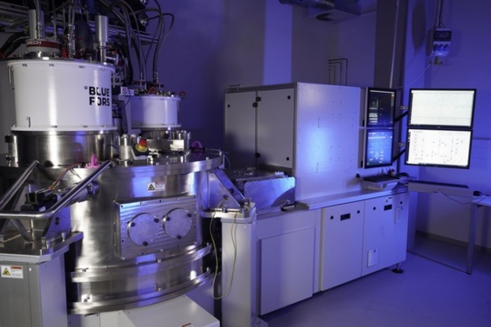
Germany’s first cryogenic measuring setup for statistical quality measurement of qubit devices on whole 200- and 300-mm wafers has started operation at Fraunhofer IAF.
With the newly set up cryogenic on-wafer prober, researchers at the Fraunhofer Institute for Applied Solid State Physics IAF aim to better understand the functioning of quantum devices based on semiconductor quantum dots and quantum wells as well as superconductors.
The device can characterise wafers in industrial sizes (200 mm and 300 mm) and high volumes (up to 25 wafers in a row) fully automatically at cryogenic temperatures below 2 K (271.15 C°).
The data sets obtained significantly reduce the dependence on random hits, which is characteristic for single measurements. In this way, the increase in measurement capacities at the institute contributes to the development of reliable production of high-quality qubits that can be used in quantum computers and quantum sensors.
At the time of commissioning, the facility is the fifth of its kind worldwide, the second in Europe and the first in Germany. The German Federal Ministry of Education and Research (BMBF) funded the procurement and installation of the wafer prober as part of the project 'KryoproPlus — Provision and Verification of a Cryogenic On-Wafer Prober.
Developing know-how for industrial qubit manufacturing
“With the on-wafer prober we gain new and unique capabilities in cryogenic characterisation nationwide,” emphasises Rüdiger Quay, KryoproPlus project coordinator and acting institute director of Fraunhofer IAF. “With this system, we will support our partners from research and industry in establishing a European supply chain for materials and production processes for solid-state qubits. This allows us to make an important contribution to the technological sovereignty of Germany and Europe,” Quay adds.
“The wafer prober provides us for the first time with statistically relevant data sets that we can use to systematically optimise and scale the production of qubit devices,” explains Nikola Komerički, who is supervising the KryoproPlus project as part of his doctorate on the characterisation of quantum computing devices. Komerički coordinated the installation and commissioning of the system and is already performing the first measurements.
“We want to better understand how to get good, homogeneous qubits to enable scaling and industrial production of qubits in Germany and Europe,” Komerički adds. “To do that, it is necessary to expand the qualitative view to include a quantitative, statistical perspective on device behavior.”
Better data through automated measurement of whole 200 mm and 300 mm wafers at temperatures below 2 K
Qubits based on semiconductor quantum dots and quantum wells as well as superconductors operate at temperatures close to absolute zero (-273.15 °C). This minimises ambient interference, activates superconductivity, and thus enables the formation and entanglement of qubits. Accordingly, it is essential for the testing, optimisation and scaling of qubits that they are characterised at their operating temperature and that a statistically evaluable set of measurement data is collected.
The cryogenic on-wafer prober closes this characterisation gap. The automated measurement of entire 200 mm and 300 mm wafers at temperatures below 2 K with a short changing time increases the amount of available data. This data provides researchers and engineers with the necessary basis to make targeted improvements to qubit-formation devices and increase scalability.
Characterisation of qubit devices in the projects MATQu, QUASAR and QLSI
With the full commissioning of the wafer prober, the project KryoproPlus has been completed. The first measurements of the facility are in the projects 'MATQu — Materials for Quantum Computing,' “QUASAR — Semiconductor Quantum Processor with Shuttling-based Scalable Architecture' and 'QLSI — Large Scale Quantum Integration with Silicon.'
For MATQu, Komerički is characterising and analysing (niobium) Josephson junctions, which are devices for transmon qubits. For QUASAR and QLSI, characterisations of FETs for single-electron transistors (SETs) based on silicon quantum wells and, subsequently, SETs that serve as devices for spin qubits are being performed.


