
LED design could enable more immersive displays
Researchers develop cheap, ultra-small LEDs for full-colour imaging at high resolution
From pterodactyls flying overhead in a game to virtually applying cosmetics prior to making a purchase, augmented reality and other immersive technologies are transforming how we play, observe, and learn. Cheap and ultra-small LEDs that enable full-colour imaging at high resolution would help immersive displays reach their full potential, but are not currently available.
Now, in a study 'RGB monolithic GaInN-based μLED arrays connected via tunnel junctions' recently published in Applied Physics Express, a team led by researchers at Meijo University and King Abdullah University of Science and Technology (KAUST) has successfully developed such LEDs. They say the simplicity of their fabrication, via presently available manufacturing methods, means they could be readily incorporated into modern metaverse applications.
The realism of augmented and virtual reality depends in part on resolution, detail, and colour breadth. For example, all colours must be evident and distinguishable from one another. GaInN semiconductors are versatile materials for LEDs that meet all of these requirements. However, constructing them as a single unit on the same substrate – rather than as separate elements – is essential for obtaining optimum performance. This is what the researchers set out to do.
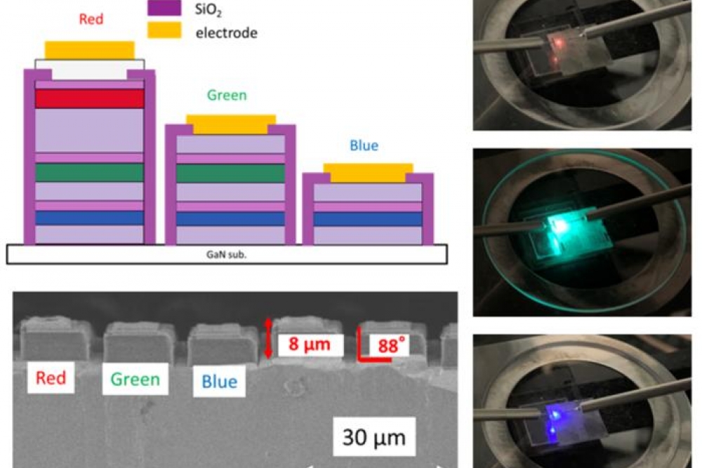
We sequentially stacked blue, green, and red micro-LED arrays – connected by tunnel junctions, based on the quantum mechanical principle of electron transport through a thin insulating layer – onto the same wafer, explains Motoaki Iwaya, senior author (Meijo). We fabricated complex mesa architectures and attained a pixel density of 330 pixels per inch.
At a current density of 50 amperes per square centimetre, the emission wavelengths of the LEDs were 486, 514, and 604 nm, respectively. The full width at half maximum of the emission spectrum is narrow enough to emit red, blue, and green light, and more than enough to distinguish between them.
There were a few extraneous emitted wavelengths, and the red and blue emissions were substantially less than the green emission – both attributable to damage during device fabrication, explains senior author Kazuhiro Ohkawa (KAUST). Optimising the crystal growth conditions should ameliorate these defects.
This work has minimised the common limitations of past LEDs based on GaInN technology. Preparing the devices on cheap sapphire substrates will be necessary for practical use, and such work is underway in our laboratory, says senior author Daisuke Iida (KAUST). We believe our work is an important step toward realistic, immersive visual experiences that require ultra-high brightness and definition.


