
Indian team makes home-grown GaN power switch
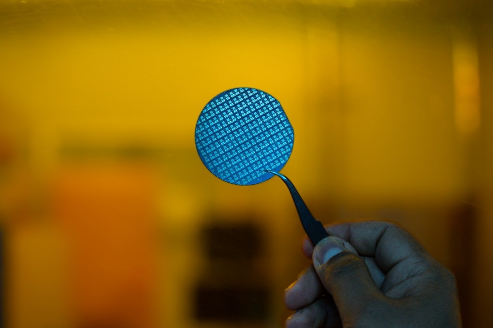
Two-inch GaN-on-silicon wafer with power transistors, developed at Indian Institute of Science
Researchers at the Indian Institute of Science (IISc) have developed a home-grown GaN power switch that can have potential applications in systems like power converters for electric vehicles and laptops, as well as in wireless communications. The entire process of building the switch – from material growth to device fabrication to packaging – was developed in-house at the Centre for Nano Science and Engineering (CeNSE), IISc.
“It is a very promising and disruptive technology,” says Digbijoy Nath, associate professor at CeNSE and corresponding author of the study published in Microelectronic Engineering. “But the material and devices are heavily import-restricted … We don’t have GaN wafer production capability at commercial scale in India yet.” The know-how of manufacturing these devices is also a heavily-guarded secret with few studies published on the details of the processes involved, he adds.
To design the GaN power switch, the IISc team used a MOCVD technique developed and optimised over a decade by researchers in the lab of Srinivasan Raghavan, professor and chair, CeNSE.
GaN transistors typically operate in depletion mode – they are on all the time unless a negative voltage is applied to turn them off. But power switches used in chargers and adapters need to work the other way around. To achieve this operation, the team combined the GaN transistor with a commercially available silicon transistor to keep the device normally off.
“The packaging of the device was also indigenously developed,” explains Rijo Baby, PhD student at CeNSE and first author of the study. After packaging and testing, the team found the device performance to be comparable to state-of-the-art switches available commercially, with a switching time of about 50 nanoseconds between on and off operations.
Going forward, the researchers plan on scaling up the device dimensions so that it can operate at high currents. They also plan to design a power converter that can step up or step down voltages.
“If you look at strategic organisations in India, they have a hard time procuring GaN transistors … It is impossible to import them beyond a certain quantity or power/frequency rating,” says Nath. “This is essentially a demonstration of indigenous GaN technology development.”
Reference
'8A, 200V normally-off cascode GaN-on-Si HEMT: From epitaxy to double pulse testing' by R Baby et al; , Microelectronic Engineering (2023)


