The three-in-one microLED
Selective removal of active layers creates a monolithic full-colour LED
Engineers from Toyoda Gosei are claiming to have made significant strides in improving the simplicity of making microLEDs for full-colour displays. Using the selective removal of active layers, they have created a monolithic InGaN LED that emits in the red, green and blue.
“We believe that this simplicity makes it possible to produce micro-displays with fine pixels at low cost,” claims team spokesman Koichi Goshonoo.
He points out that another attribute of their architecture is the common cathode, which negates complexity in the driving circuit.
Toyoda Gosei’s technology is not the only approach that realises multi-colour monolithic microLEDs. Other options include: combining blue LEDs with quantum dots that emit in the red and green; using a cascaded or stacked structure of LEDs; turning to nanowires; and adjusting the facet plane to increase indium uptake. However, according to Goshonoo and co-workers, all these alternatives are plagued by cost and yield issues, stemming from the complexity of the structure and the process.
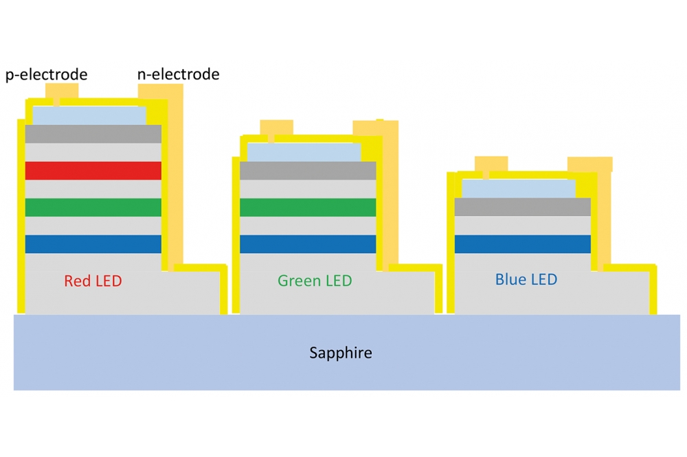
In the team’s design, the blue LED has just a blue emitting quantum well, while the green LED has green-emitting wells on top of blue variants, and the red LED has all three forms of wells (see Figure). However, in each case, emission from just one region dominates.
An explanation for the spectral purity of the emission is provided by simulations of the band diagram and carrier profiles. Such efforts have been undertaken with a LASTIP package produced by Crosslight.
Simulations show that for the red LED, there is preferential electroluminescence in the red-emitting layer. That’s partly because this layer has the smallest bandgap, but it is also a consequence of the low mobility of the holes – those injected from the p-type layer don’t travel that far, staying near the red-emitting wells. Another factor at play is that the n-type intermediate layers between the radiative regions ensure the transportation of electrons from the blue-emitting region to that emitting in the red. Similarly, the transport of holes to the green and blue light-emitting layers is inhibited, aiding pure red emission.
The same mechanisms are at play in the green LED, ensuring that it produces predominantly green emission, while in the blue LED there are just blue-emitting wells, as is the case in a conventional LED.
Goshonoo and colleagues produced their full-colour LED by loading a sapphire substrate into an MOCVD reactor and growing a GaN-based epistructure that contained three 3.5 nm-thick blue-emitting InGaN quantum wells, two 3.5 nm-thick green-emitting InGaN quantum wells and a single 3.5 nm-thick red-emitting InGaN quantum well. The team decreased the number of wells at longer wavelengths to try and limit the deterioration in quantum-well quality that occurs when increasing indium content.
Patterning and dry etching with chlorine gas enabled selective removal of regions emitting in the green and red, prior to the growth of a p-type region with an electron-blocking layer, the formation of a mesa, and the addition of a protective film and electrodes.
The emitting area, determined by the dimensions of an ITO layer, is 250 mm by 400 mm. However, smaller values are possible. “The target size of each colour sub-pixel is less than 1 µm,” says Goshonoo, who adds that 10 µm has been verified.
Luminescence characterisation revealed a wide colour gamut, with a National Television Standards Committee coverage of 95.4 percent. However, wall-plug efficiencies are a concern, with values at 20 mA of 0.17 percent in the red, 5.9 percent in the green and 0.65 percent in the blue.
Lower efficiency in the blue is blamed on the formation of non-radiative recombination centres during removal of regions developed for emission in the red and green. Optimising the process could address this issue.
Increasing the efficiency of the red LED is more challenging. “Many research institutions, including ours, are working on this issue, and we hope that it will be overcome someday,” says Goshonoo, who added that another of the team’s goals is to prototype a microLED.
Reference
K. Goshonoo et. al. Appl. Phys. Express 16 082004 (2023)


