High-power lasers: wells or dots?

When it comes to satellite communication, is it better to use high-power lasers with quantum wells or variants that employ quantum dots?
BY YONGKUN SIN FROM THE AEROSPACE CORPORATION
This decade will witness significant growth in the satellite communications market. That’s good news for the makers of high-power broad-area lasers that emit between 915 nm and 980 nm, because these sources are a critical component in space satellite communications systems. For example, SpaceX, the company led by Elon Musk, uses Starlink satellites that are equipped with laser links to help to drive down latency on the internet network for satellite broadband. Note that plans for SpaceX include using lasers on future Starlink satellites for the transmission of information between them while in orbit.
At the heart of the broad-area lasers deployed in space are strained quantum well active regions made of an InGaAs-AlGaAs heterostructure. As well as a high level of efficiency, these broad-area lasers with a single InGaAs quantum well produce unprecedented high-power operation, thanks to efforts to understand and combat causes of device failure. Investigations have uncovered the origins of facet catastrophic optical damage or catastrophic optical mirror damage in GaAs-based lasers and led to the development of techniques such as facet passivation to significantly increase the threshold for the cause of facet failure. These advances have enabled broad-area lasers with a waveguide width of around 100 mm to produce CW output powers of over 20 W. However, while this progress is very encouraging, these lasers are still susceptible to catastrophic optical damage, which can cause catastrophic and sudden degradation. That’s a major concern for space applications. So, to understand the origins of this failure, our group at The Aerospace Corporation has delved into this matter, finding that these broad-area lasers predominantly degrade by a new failure mode that’s associated with catastrophic optical bulk damage.
Figure 1.
Electroluminescence images of a quantum well laser showing self-focusing of
filaments (b) and development of dark line defects (c).
An alternative class of laser that could provide the source for satellite communication is the InAs-GaAs quantum dot laser. Recently, this emitter has attracted much attention as a potential successor to quantum well lasers in silicon photonics, with the three-dimensional confinement of carriers in the active region promising to suppress nonradiative recombination of carriers at growth and radiation-induced defect sites. This asset makes the quantum dot laser an attractive candidate for space applications. However, its failure modes and mechanisms are still not understood. To help address this lack of knowledge, we have compared the degradation processes in high-power broad-area lasers with quantum well and quantum dot active regions. Read on to discover our findings.
Device
designs
We have
studied quantum well and quantum dot lasers that share the same geometry. Both
have 2 mm-long cavities and waveguides 100 mm wide. These lasers have been
passivated and had anti-reflection and high-reflectivity coatings applied to
their facets. In addition, windows have been introduced in the backside n-metals
during the fabrication of these laser diodes, to allow us to directly observe
spontaneous emission from the entire laser cavity.
Our strained quantum well lasers, emitting between 960 nm and 980 nm, are grown by MOCVD and contain an InGaAs graded-index separate-confinement heterostructure that is sandwiched between the AlGaAs cladding layers. In comparison, the InAs-GaAs quantum dot lasers, emitting at around 1 µm, are grown by MBE, with dots formed by the Stranski–Krastanov process. These lasers contain ten stacks of InAs quantum dots.
To evaluate both our quantum well and our quantum dot window lasers, we have attached them to C-mounts, using a p-side down configuration. As the lasing wavelength of both of these lasers is transparent to the GaAs substrate, it is easy for us to observe the optical intensity distribution within the active layer through the substrate.
Figure 2.
Electroluminescence images of a quantum dot laser showing the development of
dark area defects.
Comparing
quantum well lasers…
Our
room-temperature measurements reveal that the quantum well laser has a
threshold current of 280 mA, a slope efficiency of 0.9 W/A, a peak power
conversion efficiency of 50 percent, and an external differential quantum
efficiency of 0.71. In comparison, when the quantum dot laser is measured at
room temperature it has a threshold current of 700 mA, a slope efficiency of
0.8 W/A, a differential resistance of 0.1 W, a threshold voltage of 1074 mV, and
optical output power of 3.5 W at 6 A.
Near-field profiles for the two types of lasers are markedly different. The quantum-well laser has an array of filaments, with around 10 maxima and a typical filament spacing of 10 mm. In comparison, near-field profiles for the quantum dot lasers reveal significantly suppressed filamentation. The most probable cause of this difference is that the quantum dot lasers have a much smaller linewidth enhancement factor than their quantum-well cousins.
We have undertaken accelerated life-tests, monitoring laser diode parameters, such as optical power, current and voltage, for a range of heatsink temperatures. This has allowed us to determine aging behaviour – be it rapid, gradual, or catastrophic/sudden – and failure times.
To gain insight into degradation processes in both types of lasers, we have also captured electroluminescence images from the window regions in real-time during the entire life-tests until device failure. With this technique, offering a nominal spatial resolution of 2 mm/pixel, we typically collect one electroluminescence image per second for the duration of the life-tests. These images allow us to observe quite a few critical events in real time, including self-focusing of filaments, formation of dark spot and dark line defects, and the propagation of dark line defects.
Snapshots of time-resolved electroluminescence images from our quantum well laser are shown in Figure 1. We drove this laser under continuous-wave operation at 6 A, using a heatsink temperature of 70 °C. Comparing images at times t = 0 and t = t1, it is easy to spot the precursor signature of failure – self-focusing of filaments, indicated by the dotted white arrow.
This self-focusing, which causes the filaments to converge via thermal lensing, stems from local gain saturation and spatial hole burning. We find that the optically induced heating that results from self-focusing of filaments significantly increases the temperature within a localised area, thus forming a hot spot. Our electroluminescence images indicate that dark line defects develop at that location at t1 + 9 s (the initiation point of these defects, shown in Figure 1 (c), is highlighted by the dotted white arrow). As the dark line defects develop, the power produced by the laser reduces significantly.
During device operation, pre-existing point defects in the active layer are transformed into defect complexes via a recombination-enhanced defect reaction process. During this process, the point defects migrate, react, and dissociate. This degradation comes from a defect reaction that is enhanced by the non-radiative recombination of carriers. Note that the non-radiative recombination processes at the sites of non-radiative recombination centres generate thermal gradients during device operation.
One of the consequences of nonradiative recombination is that it leads to local heating, which subsequently increases optical absorption. Assuming an absorption coefficient of 200 cm-1 with no local heating in the quantum well lasers, the absorption coefficient increases to 8.7 x 104 cm-1 for local heating of 130 °C. Local heating of 130 °C is one of the three critical temperatures prior to quantum well laser degradation. We have found that when the local temperature reaches around 130 °C, the local area begins to strongly absorb lasing photons. In turn, filamentation and self-focusing of filaments resulting from local gain saturation and spatial hole burning start to play a critical role.
Another impact of local heating is that it creates a thermal lens, which also leads to local gain saturation. The thermal lens can cause a narrowing and self-focusing of the optical beam as it propagates, leading to a significant increase in the local optical power density (see the dotted white arrow in Figure 1 (b)). As thermal lensing can further enhance the self-focusing of filaments as they propagate along the longitudinal axis, it is likely that the optical intensities at local areas critically depend on thermal gradients.
When a local temperature rise exceeds 130 °C, the hot spot created by the optically induced heating can accelerate the recombination-enhanced defect reaction process and cause nonradiative recombination centres to develop into extended defects. Another event occurs when local heating increases beyond 300 °C, with the increase in the absorption coefficient reaching of 2.5 x 108 cm-1, and a thermal runaway process commencing. This thermal runaway process may lead to local melting in the quantum well lasers when local heating reaches as high as 1200 °C. However, local melting is not a prerequisite for the generation of extensive dislocation networks.
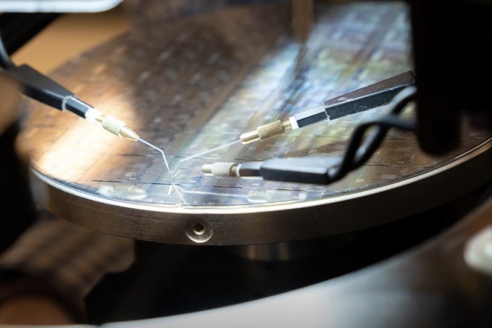
Emily Tang, a research associate at The
Aerospace Corporation working on the time-resolved electroluminescence set-up.
…and
quantum dot lasers
We have
also carried out accelerated life-tests on quantum dot lasers, using automatic
current control, with our time-resolved electroluminescence set up (see Figure
2 for images captured from one of the quantum dot lasers).
Driving this particular laser at 6.5 A and a heat-sink temperature of 75 °C, we have determined that the first sign of change is a weakly damaged area (indicated by the dotted yellow rectangle in Figure 2 (b), taken at t = t1, and its absence in Figure 2(a), taken at t = 0). There is no evidence of any precursor signature of failure, such as self-focusing of the filaments. This clearly indicates that optical effects are less critical in quantum dot lasers than quantum well lasers, where they are to blame for forming dark line defects. However, electrical and thermal effects appear to be more critical for quantum dot lasers.
Driving quantum dot lasers for longer creates more regions of damage. Each of the electroluminescence images in Figure 2 (c) to 2 (i) has two dotted rectangles, coloured with yellow and orange to indicate original and newly damaged areas, respectively. We have three noteworthy observations from these electroluminescence images: newly damaged areas were mainly developed towards the rear facet; over 7 days the length of newly developed dark area defects increased from around 60 mm to 235 mm; and the patches of weakly damaged areas, or less dense dislocations, became significantly denser over 7 days.
To fully understand the nature of these dislocations, we would need to prepare transmission electron microscopy specimens from a series of quantum dot lasers at different stages of degradation. While that’s our future work, we can still suggest a scenario for the degradation: there is a recombination-enhanced defect reaction process that generates dislocations (shown as the weakly damaged area in Figure 2 (b)) from nonradiative recombination centres and point defects in the quantum dot active region. These dislocations slowly propagate via a recombination-enhanced dislocation glide process, shown in Figure 2 (c) – (i). The propagation velocity for this process is much slower than that of dark line defects in quantum well lasers.
Wells
versus dots
Our efforts
have shown that broad-area lasers with quantum well and quantum dot active
regions undergo very different degradation processes. In quantum well lasers,
dark line defects form by precursory self-focusing of filaments, thus forming a
hot spot; while in quantum dot lasers, dark area defects form with no precursor
signature of failure. However, there is common ground, with quantum well and
quantum dot lasers showing bulk failures – the former by fast catastrophic
optical bulk damage and the latter by slow gradual degradation, possibly via a
recombination-enhanced dislocation glide process. Further studies are necessary
to fully understand degradation mechanisms in quantum dot lasers, but merits of
quantum dot lasers articulated in this article may warrant these lasers in
future space satellite systems.
Further reading
Y. Sin et al. “Catastrophic optical bulk damage in high-power InGaAs-AlGaAs strained quantum well lasers,” IEEE Journal of Selected Topics in Quantum Electronics 23 1500813 (2017)
Y. Sin et al. “Degradation in high-power broad-area lasers with quantum well and quantum dot active regions: a comparative study,” Proc. SPIE 12403 124030C (2023)


