Aixtron tool helps BelGaN expand GaN business

European semiconductor foundry invests in G10-GaN MOCVD system to expand business
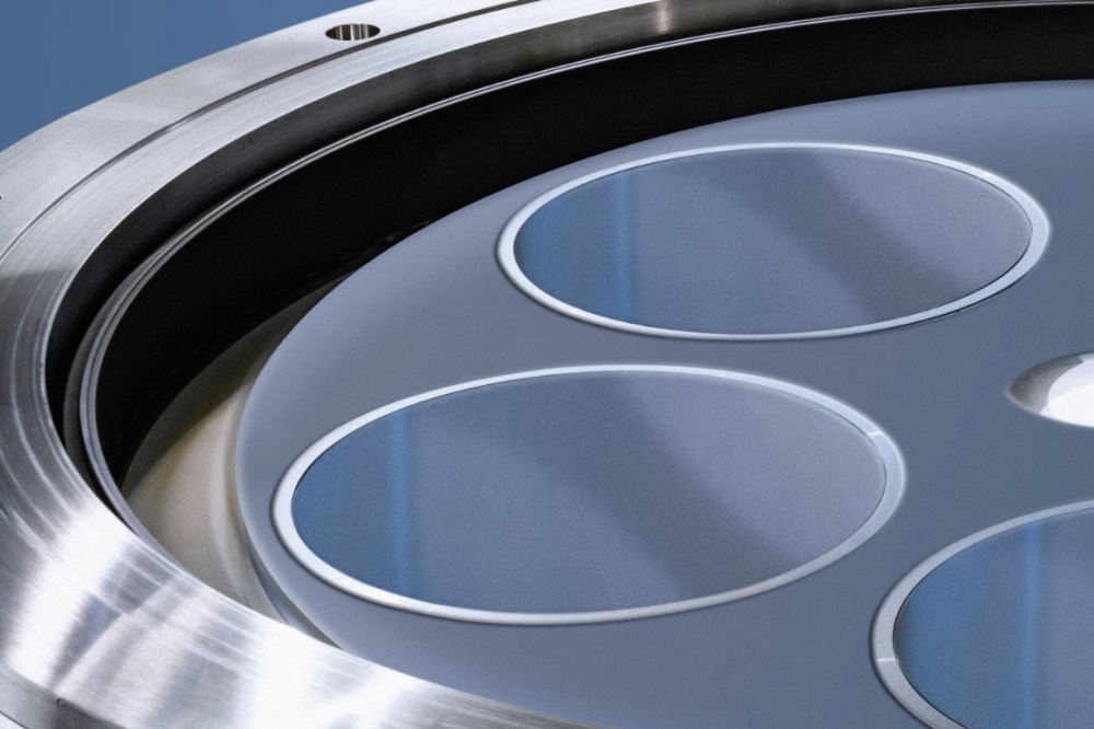
European semiconductor foundry BelGaN will be using Aixtron’s new G10-GaN MOCVD tool to expand its business into the growing GaN market.
Starting with an 8x150mm configuration, the system will be delivered to the BelGaN production site in Oudenaarde (Belgium) before the end of 2023 and will in the future migrate to 5x200mm.
BelGaN, a GaN automotive-qualified semiconductor open foundry, recently announced the production start of its first generation 650V eGaN technology. The Gen1 platform is designed for the requirements of energy-efficient applications for sustainability and carbon neutrality, according to Aixtron.
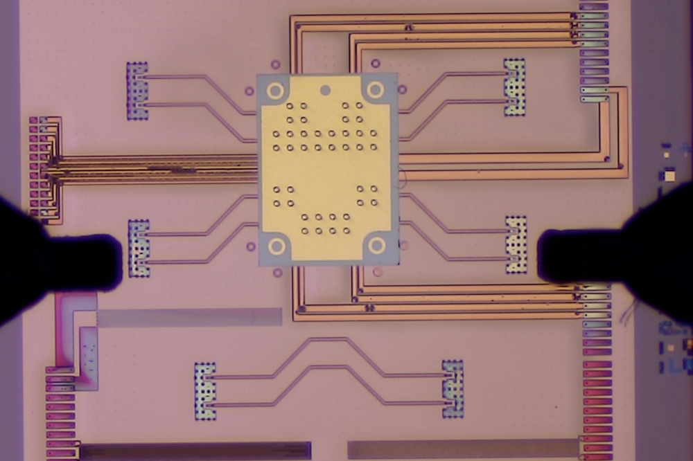
The G10-GaN will be used to further extend the range of power chips with voltage ratings from 40V to 1200V, using GaN-on-Si, GaN on SOI, and novel GaN-on-engineered substrates. It will be applied both on lateral as well as vertical power-GaN products, with a focus on high performance, automotive quality and reliability, high yield, and low costs.
GaN-epitaxy using MOCVD is a critical process in any power-GaN technology, both to innovate device architectures, boost performance, yield, and quality, and to cut down the cost of GaN products. according to Marnix Tack, CTO and VP business development of BelGaN. "We have been impressed by the high levels of productivity, uniformity, and low cost of ownership of Aixtron’s new G10 platform," he said.
The new G10-GaN cluster solution builds on the fundamentals of Aixtron’s current tool the G5+ C, while delivering twice the productivity per cleanroom area. The G10-GaN also guarantees the highest throughput per m2/cleanroom, and with its full automation end-to-end, it is the only MOCVD system fully designed for silicon fabs.


