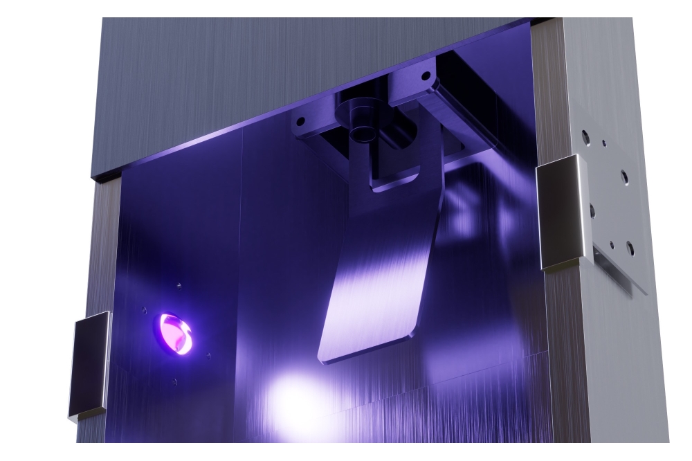
Imec's GaN-on-silicon HEMTs target 5G base stations

At the 2023 International Electron Devices Meeting (IEEE IEDM 2023), imec presented a paper on AlN/GaN MISHEMTs on 200mm silicon with high output power and energy efficiency while operating at 28GHz. With these results, imec's GaN-on-silicon MISHEMT technology outperforms other GaN MISHEMT device technology in terms of performance, while the adoption of the silicon substrate provides a major cost advantage for industrial manufacturing.
GaN based (MIS)HEMTs are widely explored for 5G-advanced high-capacity wireless communication applications, the next evolutionary step in 5G technology. Due to their outstanding material properties, GaN-based devices offer superior performance over CMOS devices and GaAs HEMTs in terms of output power and energy efficiency. Industry is looking at two different RF use cases: (1) mobile devices where GaN (MIS)HEMTs are used in power amplifier circuits operating at relatively low voltages (i.e., VDD below 10V); and base stations where VDD voltages are higher (above 20V). For the latter case, GaN-on-SiC devices offer the largest potential, but SiC substrates are expensive and small in size. The ability to integrate GaN HEMTs on silicon offers a tremendous cost advantage and potential for technology upscaling, but the performance of GaN-on-silicon based (MIS)HEMTs lags behind.
“The challenge is in achieving a high operating frequency (derived from the fT and fmax at small-signal conditions) while at the same time delivering a high output power with sufficient efficiency (derived from the devices large-signal performance),” explains Nadine Collaert, imec fellow and program director advanced RF at imec. “While most GaN devices are HEMTs, in this experimental study, we focused on GaN-on-silicon MISHEMTs with AlN barriers as a crucial step towards addressing the demand for both high-power D-mode devices for infrastructure as well as low-voltage e-mode devices required in mobile handsets. These GaN MISHEMT devices, featuring a relaxed gate length of 100 nm, demonstrate exceptional performance across various metrics. Specifically, for low-voltage (up to 10V) applications, these devices achieved a saturated output power (PSAT) of 2.2W/mm (26.8 dBm) and a power added efficiency (PAE) of 55.5% at 28 GHz, positioning our technology better than comparable HEMT/MISHEMTs out there. These results underscore the potential of our technology as a strong foundation for next-generation 5G applications.”

Large-signal performance benchmarking (at 28-40GHz) for GaN MISHEMTs, MOSHEMTs and AlN/GaN HEMTs integrated on a silicon substrate. The graph shows PAE vs. PSAT normalized with gate width (W/mm). [1] H. W. Then, IEDM, pp. 402-05, 2019; [2] H. W. Then, IEDM, pp. 230-233, 2021; [3] P. Cui, Semi. Sci. Tech., 38 035011, 2023; [4] H. Du, EDL, vol. 44, no. 6, pp. 911-14, 2023; [5] E. Carneiro, Electronics, 12(13), p. 2974, 2023; [6] H. W. Then, VLSI 2020.
Also, for base stations (20 V applications), excellent large-signal performance at 28 GHz is demonstrated with a PSAT of 2.8W/mm (27.5dBm) and PAE of 54.8%. “Our AlN/GaN MISHEMTs are still D-mode devices,” adds Nadine Collaert. “But we know the path towards E-mode devices, through further device stack engineering.”
Underlying the performance improvement is a comprehensive study of the impact of the thickness scaling of the AlN and Si3N4 layers, which are used as stop barrier layer, and also gate dielectric, respectively. Ultrathin stacks, for example, enable a high operating frequency, but come at the expense of trapping-induced current collapse and device breakdown in large-signal conditions. A broader study of on-state breakdown of GaN HEMTs, also shown at IEDM, reveals the mechanism behind these reliability issues. “These fundamental studies give us a modelling platform to further optimize the design of our GaN-based material stack for specific use cases,” adds Nadine Collaert.