The case for better templates
Higher-quality AlN-on-sapphire templates are need to improve the performance of deep-UV LEDs
Researchers at the University of California, Santa Barbara, say that better templates are needed to improve the performance of the deep-UV LED.
A common platform for this light source, which is an attractive option for disinfection applications, is the commercial AlN-on-sapphire template. However, the quality of this template can limit the thickness of the n-type AlGaN layer within the LED, thereby impacting the sheet and series resistance and ultimately dragging down the device’s wall-plug efficiency.
“With the current threading dislocation densities offered from commercial AlN-on-sapphire templates, thick n-AlGaN growth beyond 800 nm is problematic due to threading dislocation inclination,” explains team spokesman Michael Wang.
He claims that reducing the threading dislocation density of commercial templates by an order of magnitude would enable much thicker n-AlGaN films, and thus better voltage efficiency at higher currents.
According to Wang, commercial devices tend to operate at more than 20 A cm-2. “If a thin n-AlGaN layer is used, the wall-plug efficiency will be limited at these current densities,” remarked Wang.
Yet another benefit of higher-quality templates is that they increase the internal quantum efficiency of the LED, thanks to a reduction in non-radiative recombination in the active region.
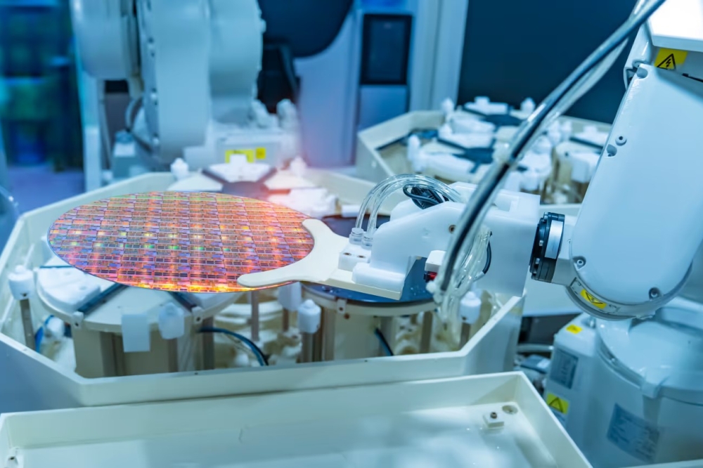
The study by Wang and co-workers involved growth by MOCVD of deep-UV epistructures on commercially available AlN-on-sapphire templates. On these templates the team added a 70 nm-thick Al0.85Ga0.15N buffer and a 400 nm-thick silicon-doped Al0.65Ga0.35N layer, using a low III-V ratio to improve conductivity and morphology. These layers were followed by a lightly doped smoothing superlattice, an active region with six 1.5 nm-thick Al0.5Ga0.5N quantum wells, an electron-blocking layer, a p-type superlattice and a p-contact layer.
The team also produced several n-type AlGaN samples, formed by keeping silicon-doping in the Al0.65Ga0.35N layer at 5 x 1019 cm-3 and increasing thethickness. According to atomic force microscopy scans of 2 mm by 2 mm areas of these samples, increasing the thickness of the Al0.65Ga0.35N layer from 400 nm to 1600 nm led to an increase in root-mean-square roughness from 3.4 nm to 22 nm. This far higher roughness resulted from the presence of large hillocks.
Reciprocal space mapping of the samples using X-ray diffraction revealed that when the Al0.65Ga0.35N layer is 400 nm-thick it is fully strained, but when the thickness is increased to 800 nm and 1600 nm it is 38 percent and 100 percent relaxed, respectively. The X-ray diffraction-based technique also determined that as the thickness of Al0.65Ga0.35N increases, there is a compositional drift to higher gallium content, possibly due to a compositional pulling effect.
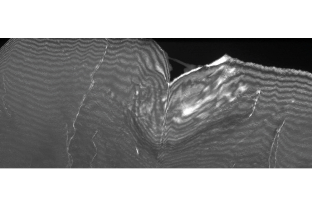
The team scrutinised the material quality of their samples with transmission electron microscopy. Those with a thicker Al0.65Ga0.35N layer had cracks that led to the nucleation of new threading dislocations.
Based on the characterisation techniques employed, Wang and co-workers concluded that for today’s templates, which have threading dislocation densities between 5 x 108 cm-2 and 5 x 109 cm-2, it’s critical to keep the thickness of the n-AlGaN layer below the threshold where tensile strain from threading dislocation inclination induces morphological degradation and compositional drift. They point out that templates with a lower threading dislocation density can increase the cracking limit, decrease compositional pulling and the rate of n-AlGaN decomposition, and ultimately enable an increase in the thickness of this layer, leading to better devices.
UV LEDs produced during this study are claimed to be comparable to state of the art. Emitting with a peak wavelength of 285 nm, these devices produce a peak external quantum efficiency (EQE) of 10.6 percent at a current density below 1 A cm-2.
“The key limitation to UV LEDs at this point in time is light extraction,” says Wang. “Our group, along with many others, is hitting a wall at around 10-20 percent EQE, because the light extraction from AlN on single-side-polished sapphire is around 20 percent at the most.”
Pictured above: Cross-sectional transmission electron microscopy uncovers cracks in thicker layers of n-AlGaN.
Reference
M. Wang et al. Appl. Phys. Lett. 123 2311010 (2023)