Advancing vertical GaN diodes
Optimising doping with a foundry-compatible process produces vertical p-i-n diodes with avalanche behaviour
There are many merits of vertical GaN p-i-n diodes grown on native substrates, including a simple architecture, low leakage and a high breakdown voltage.
While high-volume production of these devices is hampered by the absence of a foundry process, progress on this front is being made by a collaboration between Vanderbilt University, the Naval Postgraduate School, the Naval Research Laboratory and Sandia National Laboratory.
This US team is pursuing a foundry-compatible planar process that controls the electric field and prevents current crowding by managing the dose in the anode extension region. Building on previous work that reported how the dose depends on the thickness of the anode, they are now unveiling the relationship between the dose and the anode doping level.
Commenting on their findings, Mona Ebrish from Vanderbilt University remarks: “The devices with a moderate anode doping have performed the best, and our TCAD simulation shed some light on the reasoning behind our experimental finding.”
She believes that the approach they have adopted, involving a combination of experimental analysis and simulation, could be extended to other device designs.
A highlight of this study is that in one of the diodes the team recorded avalanche breakdown at different temperatures, a trait indicative of a non-destructive process.
The researchers also found that current increases as function of temperature, leading to a higher breakdown voltage. According to Ebrish, this behaviour suggests successful management of the electric field in the device, an asset not found in all p-i-n diodes: “Often devices either do not respond to the increase in temperature, or they experience a surge in current and burn – destructive breakdown.”
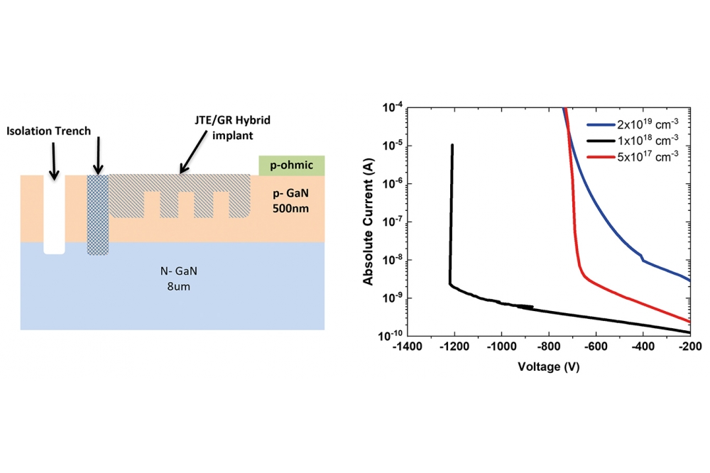
The team produced their devices by loading non-homogenous GaN substrates into an MOCVD reactor and growing 500 nm-thick anode layers with magnesium doping levels of either 5 x 1017 cm-3,1 x 1018 cm-3 or 2 x 1019 cm-3. For all three samples, which have a 8 µm-thick lightly doped drift layer with a doping concentration of 1-2 x 1016 cm-3, thermal annealing at 900 °C activated the anode dopants.
To form devices from the epiwafers, the team employed an edge-termination process that involved: etching a 1 µm-deep trench about 140 nm from the anode edge; applying a nitrogen implant with a box profile, using three different energies and a total depth of 650 nm; and using a nitrogen implant to define the junction termination extension and the guard rings (see figure for the architecture of the device). To completed the fabrication of the diode, the team added a Pd/Pt/Au stack for the p-GaN anode and a Ti/Al/Ni/Au stack for the cathode.
Electrical measurements on the three devices uncovered significant differences in breakdown voltage and leakage current, despite the identical drift layer thickness, doping level and edge termination process. The variant with anode doping of 1 x 1018 cm-3 exhibits a sharp breakdown at 1.2 kV, implying superior field management in the anode extension region. It is argued that the other two devices do not exhibit the same breakdown behaviour because the extension region is not fully depleted of charges, with the remaining charges to blame for premature breakdown.
The team also carried out avalanche tests, involving temperature-dependent reverse sweeps at 25 °C, 100 °C, 150 °C and 200 °C. They found that devices with doping levels of 5 x 1017 cm-3 and 2 x 1019 cm-3 struggled to avalanche, due to high leakage and an inconsistent trend with temperature, while the p-i-n diode with a doping of 1 x 1018 cm-3 avalanched, with an increasing breakdown voltage of 10 V for every 50 °C.
Ebrish says that further improvement to device performance could come from optimising the ion-implantation process. “We are also evaluating the same process for GaN p-i-n diodes that are rated for higher voltages, like 3 kV or 6 kV.”
Pictured abofve: The p-i-n diodes produced by the team (left) have breakdown characteristics that show a tremendous variation with doping level (right).
Reference
M. Ebrish et al. Appl. Phys. Express. 16 116501 (2023)