Soctera improves GaN HEMT thermal performance

Devices exhibit a peak surface temperature rise of just 59degC while dissipating 10.4 W/mm
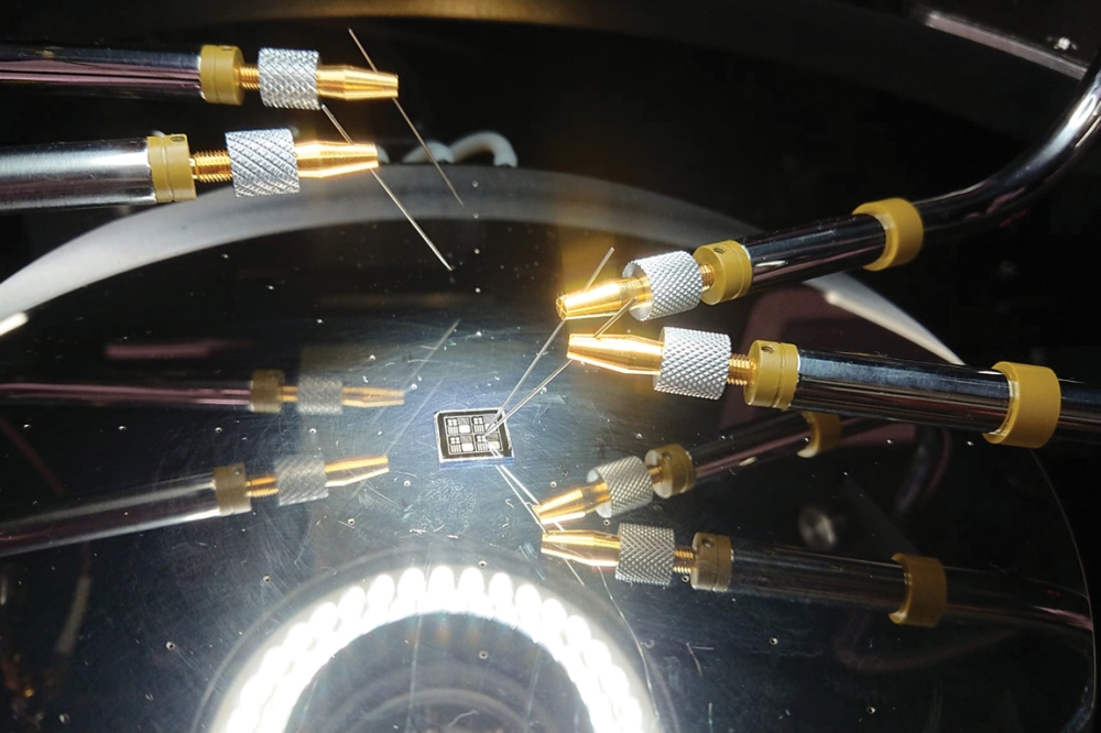
Soctera, a US developer of III-nitride power amplifiers, has demonstrated HEMTs exhibiting a peak surface temperature rise of just 59degC while dissipating 10.4 W/mm.
Typical GaN HEMTs reach the standard operating temperature limit of 225degC when dissipating approximately 5 W/mm. This dramatic improvement in thermal performance could substantially reduce thermal solution costs, enhance reliability, and increase peak power output in next-generation telecommunications (5G and beyond) and defence radar arrays.
"Reduced heat buildup redefines what is possible for the high-performance communications industry," said Soctera CEO Austin Hickman. "We are delighted with these third-party results and are working now to quickly scale our technology via commercial production methods."
Built on a thermally-optimised III-nitride material stack fully compatible with standard GaN foundry processes, Soctera's HEMTs are said to use 20x less gallium per device, which insulates Soctera's products from supply chain disruptions or price increases arising from potential future restrictions of gallium supply from China.
The HEMTs were fabricated at the Cornell Nanoscale Facility and the surface temperature profile was measured with sub-micron resolution via thermoreflectance by Microsanj, LLC.
The 4-inch wafers used in the tests were produced by IQE, with whom Soctera has partnered for commercial-scale development. Towards building out end-to-end commercial manufacturing, Soctera has started HEMT fabrication with a DoD-approved GaN foundry.
Soctera's technology maturation efforts were recently bolstered with $750,000 in non-dilutive funding awarded by the Defense Business Accelerator pitch competition.
The technology is licensed to Soctera by Cornell University, where it was initially developed at the School of Electrical and Computer Engineering.