Uncovering the secrets of SiC epilayers
Comprehensive characterisation of SiC layers is accomplished with an enhanced form of Fourier transform infra-red spectroscopy.
BY ESZTER ÉVA NAJBAUER FROM SEMILAB
Technology continues to progress, influencing our daily lives and impacting humanity’s efforts to preserve our environment. Against this backdrop, one force for good is the electric vehicle (EV), which benefits from modern power devices; these vehicles are six times more energy-efficient than those incorporating a combustion engine. But not all advancing technologies are good for the ecosystem. The acceleration in the data that is generated online every second contributes significantly to carbon dioxide emissions. Here, power supplies are required to run continuously, while demanding efficient cooling and significant storage space.
At first glance, these two domains – EVs, and the power supplies for maintaining the internet – appear to be disparate. But they share common imperatives, which are the pursuit of a higher efficiency and greater reliability through further improvement to one key component: SiC.
For high-power applications, SiC is superior to silicon on several fronts. Thanks to its high performance-to-size ratio, its greater energy efficiency, its low switching losses and its long lifetime, systems based on SiC are lighter, charge faster, and have fewer components. All these factors are valued by the EV industry. Additional benefits include high operating frequencies and temperatures, a low thermal expansion and a high thermal conductivity that reduces cooling requirements. These are strengths that deliver a huge advantage when SiC devices are deployed in data centres.
EVs and server parks are just two examples of the many ways in which SiC is making an important contribution to our daily lives. Due to its remarkable properties, there is an ever-growing demand for these compelling devices, which are amplifying waves of continuous technological improvement.
Price, however, is still a bottleneck in many SiC applications. Based on figures from May 2023, the cost of a single SiC MOSFET inverter is double that of a silicon IGBT with an equivalent performance (that is for transistors capable of withstanding 1200 V and delivering 200 A). Accounting for the lion’s share of the cost of the SiC MOSFET is its native substrate, indicating that high value is added early in the process. Due to this, it is vital to closely monitor each step in the process flow while developing highly stable production technologies. It is the norm for substrates to undergo rigorous inspection steps focusing on geometric properties, resistivity, defect assessment, surface roughness, and crystal orientation, and for epi wafers to be monitored for their epilayer thickness, doping concentration, level of defects, degree of surface roughness, and for any presence of contamination.

Figure 1. Measurements with a Michaelson interferometer involve
reflection of infra-red light from an epitaxial sample. Infrared light
is reflected off the top of the epilayer as well as the interface
between two layers (epi-substrate or epi-buffer). Interference of these
two rays enables the epitaxial layer thickness to be calculated.
A critical determinant of performance and functionality is the thickness of the epitaxial layer. This directly governs crucial electrical parameters, such as junction capacitance, and impacts several parameters in the fabrication process, including etch rates. As one of the key roles for the epilayer is to isolate the current-carrying components of the device, even small variations in epilayer thickness can have profound repercussions on the performance of diodes and MOSFETs.
To fulfil the growing demand for SiC power electronics, while executing high yields and retaining competitiveness, manufacturers of these devices are having to address the challenge of migrating from 150 mm to 200 mm wafers while maintaining uniformity in both layer thickness and electrical properties.
Often optical monitoring techniques are chosen for measuring the thickness of SiC epitaxial layers. They include Fourier-transform infrared (FTIR) reflectometry, a non-destructive technique that provides fast and accurate values for epitaxial thickness from the sub-micron to several-hundred-micron range, while avoiding risks of additional defects and contamination.

Figure 2. Interferogram of 5 µm (a) and 12 µm (b) SiC epi-samples. Fits of the sideburst maxima are shown in black.
Principles of FTIR
FTIR is a non-contact measurement technique that provides the the semiconductor industry with a wealth of information. Its capabilities include industry-standard rapid interferogram measurements of epitaxial thickness, reflectance spectrum measurements for multilayer analysis and dielectric composition measurements, and transmission measurements for absorption peak analysis.
At the heart of every FTIR spectrometer is a Michaelson interferometer (see Figure 1), which consists of a beam splitter and two mirrors: one is moveable and the other static. The position of the moving mirror is changed gradually when measuring a sample. Measurements are made of the light transmitted through and reflected from the sample. Detected signals create interferograms, with the intensity of outcoming light a function of the moving mirror’s position. For every point in the interferogram, all wavelengths in the spectrum are monitored simultaneously.
Metrology methods
Although a typical SiC epitaxial structure consists of only a high-resistivity SiC epilayer and a buffer layer on a low-resistivity substrate, there can still be large variations in layer thickness, dopant concentration, and the number of layers. When analysing any sample, its architecture will influence the most suitable method of analysis, which will also be governed by the most important characteristics to uncover.
At Semilab, we produce FTIR-based Enhanced Infrared (EIR) systems that offer a choice of three different analysis methods. Each has different capabilities and advantages for SiC epitaxial thickness measurements. We now consider, in turn, these three methods: interferogram subtraction, fast Fourier transformation (FFT), and optical modelling.
Interferogram subtraction is a widespread, robust method for determining the thickness of the epilayers. Quick and easy to set up, this approach provides information on a single layer’s thickness. Analysis is based on determining the position of the interferogram’s secondary maxima, known as sidebursts. These arise when the optical path difference between the interferometer’s mirrors matches the path difference of the rays reflected from the top of the epilayer and the epi-substrate interface. The thickness of the epilayer is proportional to the sidebursts’ position, and is easy to calculate by taking into account the sideburst position, the incidence angle of the infra-red light, the wavelength of the laser, and the refractive index of the sample.
It should be noted that it is more challenging to analyse interferograms for SiC than silicon. Due to wavelength dispersion in SiC, there are several secondary maxima in the interferogram. So, to ensure reliable analysis, there is a need for post-processing of the interferograms.

Figure 3. Baseline fringes in the reflectance spectrum of a SiC
epi-sample (top), and the thickness peak obtained by FFT (bottom).
Spectra were measured on a regrown epi-sample in collaboration with
Fraunhofer IISB, Erlangen. The FFT result shows two peaks: a total
thickness peak at around 23 µm, and a peak at the thickness of the top
epilayer, at around 11 µm. The thickness of the bottom epilayer, around
12 µm, can be obtained as a difference of the two.
Our software is more than up to this task, providing advanced SiC interferogram analysis features, including filtering, as well as various algorithms for finding and fitting maxima/minima. Depending on the sample structure, our tools for interferogram analysis may also be used to determine the total thickness of the layers for multilayer samples. However, we advise validation of the results by other analysis methods. An example of interferogram analysis of two epi structures to determine the total thickness of the buffer and the epilayer is shown in Figure 2.
More details of the epi structure can be uncovered in reflectance spectra by considering details in characteristic baseline oscillations, also referred to as fringes, that arise from interference of light reflected from each layer’s surface. It is these baseline fringes that ‘encode’ thickness information in the reflectance spectrum. Thickness values can be extracted from reflectance spectra in a fast and unambiguous manner by undertaking FFT of these fringes. As a result, we obtain the frequencies present in the signal. These can easily be converted into thickness values using the refractive index of the layer in question. For a one-layer epistructure, FFT produces a single peak that reveals the layer thickness, while measurements on multi-layer samples may produce several peaks, including those uncovering the total thickness of the stack.
To illustrate this point, see the FFT analysis of a two-layered regrown epi-sample (see Figure 3). There are two peaks, corresponding to the total thickness and the thickness of the top layer. Subtracting one from the other provides the thickness of the bottom layer.

Figure 4. Reflectance spectrum of a SiC epi sample, with the four spectral regions marked with different colours. Blue: 500-700 cm-1 shows thickness oscillations. This region is most sensitive to the effect of dopant concentration. Red: 700-1000 cm-1 is the reststrahlen band, a highly absorptive region. Green: 1000-1500 cm-1 is a transient region between an absorptive and a transparent region. 1500- cm-1 is a transparent region showing thickness oscillations.
While FFT is great way to get quick information on epiwafer thickness, using analysis that’s easy to undertake, this technique has some limitations. For samples with several layers, the result is ambiguous, in terms of the order of the layers. Another downside is that the baseline curvature in the SiC reflectance spectra causes a strong artefact to appear close to zero thickness that may obscure peak(s) of interest. Due to this issue, FFT analysis has to be restricted to samples with relatively thick epilayers, such as more than 2-3 µm.
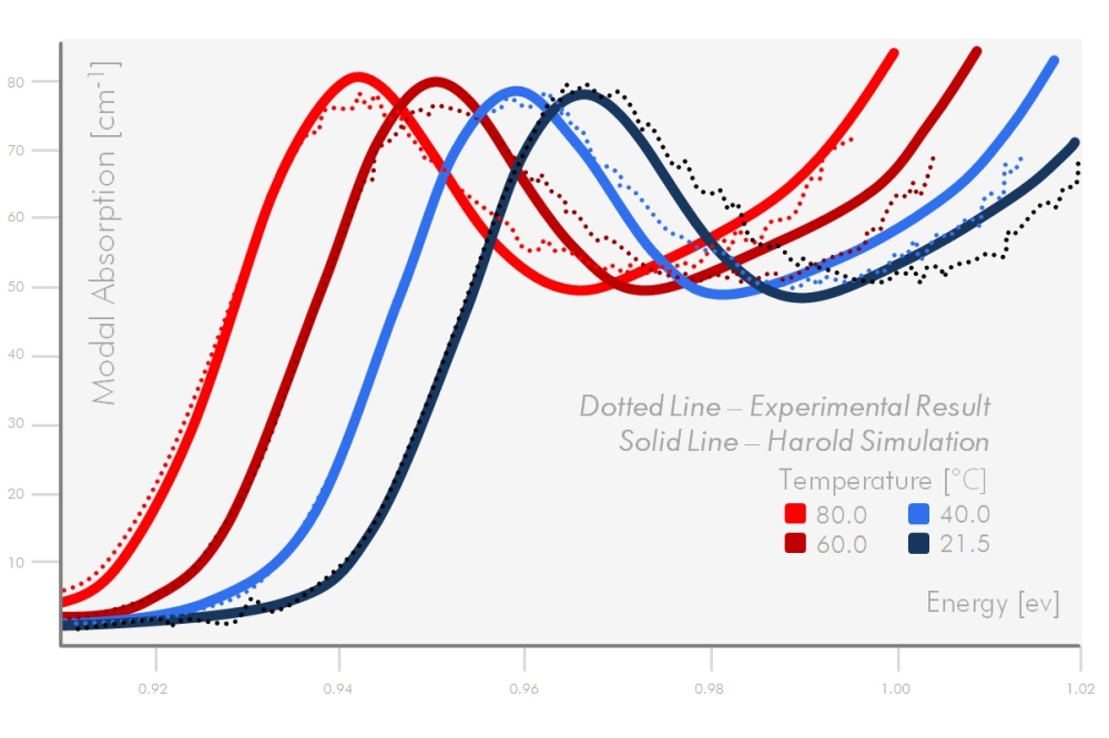
Compared with the other two techniques, interferogram subtraction and FFT, optical modelling is the most comprehensive. This approach begins by making assumptions of a structure, using estimated thicknesses and dopant concentrations. From this starting point, a reflectance spectrum is predicted, using physical laws. Depending on the modelling approach, this may involve the use of the Drude dispersion law, employed to model the effect of free-carrier concentration and using Lorentzians to model the background. By changing input parameters, one can fit the predicted spectrum to the measured reflectance spectrum, and extract important information related to the characteristics of the epilayers.

Figure 5. Structure of a typical SiC epi-sample with a 0.4 µm buffer layer (phase 1) and a 1.7 µm epi layer (phase 2).
There are four distinct regions in the SiC reflectance spectrum, each sensitive to different layers and parameters (see Figure 4). Between 400-700 cm-1 there are thickness oscillations associated with the epitaxial structure, and this is the region most sensitive to free-carrier absorption. Next to this is a spectral domain known as the reststrahlen region, spanning 700-1000 cm-1, where high levels of absorption occur for wide bandgap semiconductors. This part of the SiC reflectance spectrum is most sensitive to the top layer of the sample. Beyond this, from 1000-1500 cm-1, is a transient region, positioned between a highly absorptive and a transparent one. In the transparent region above 1500 cm-1 thickness oscillations dominate the spectrum.
If FTIR measurements are to differentiate between different layers, there has to be sufficient contrast between their optical properties. Often this contrast stems from a difference in doping – according to the Drude model, a layer’s absorption coefficient changes linearly with free-carrier concentration. However, contrast can also come from partial amorphization of a layer, originating from ion implantation. Depending on the sample’s optical characteristics, optical modelling can extract multiple layer thicknesses, such as those of the buffer and multiple epilayers, as well as higher dopant concentrations from the reflectance spectrum.
Another strength of optical modelling is that, unlike the other two methods outlined, this technique can accurately measure layers as thin as a few hundred nanometres. Care is needed, however, since in a simultaneous fit of multiple parameters correlation may appear between them, so models must be validated with repeatability and map measurements.

Figure 6. (a) Fit of a thin epiwafer’s reflectance spectrum. The measured spectrum is shown in light red, the fitted spectrum in dark red. The goodness of fit is R2=0.9995. (b) Statistics of a 15-fold centre repeat measurement. Wafer maps with (c) total, (d) epi, and (e) buffer thickness obtained by optical modelling.
To illustrate the capability of optical modelling, let us take a look at results obtained with a typical SiC epi structure (see Figure 5 for the structure, and Figure 6 for: (a), the reflectance spectrum’s fit; (b), the statistics of a centre repeat measurement; and (c), thickness maps). For this thin two-layered sample, optical modelling provides the only way to accurately determine the thickness of both the layers.
Due to ion implantation inducing partial amorphization, results of optical modelling that draw on FTIR measurements can uncover the depth of these implants. This is illustrated in Figure 7, which shows the reflectance spectrum of an ion-implanted epi structure. The spectrum contains low-frequency oscillations associated with the amorphous layer on the sample surface, as well as high-frequency oscillations, stemming from the epilayer.
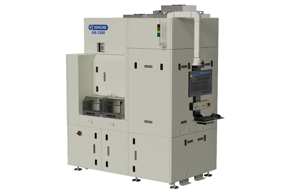
Semilab’s new FTIR metrology system
To ensure effective SiC device manufacturing, there is a need for accurate metrology, supported by seamless in-line integration features. Offering all this and more is our EIR-2300. This tool, designed for fully automated SiC fabs, has the smallest possible footprint, allowing back-to-back or to-the-wall placement. Configured with a mini environment and a faster robot for higher troughput, it has verstile loapdort and automation configuration, including standard mechanical interface (SMIF) or open cassette loadports, and overhead hoist transfer (OHT) or automated guided vehicle (AGV) compability. The EIR-2201 and EIR-2202 are economical alternatives with manual loadports and an AGV option, or a SMIF loadport with an OHT or an AGV option.

Figure 7. Optical modelling of an ion-implanted epiwafer. The thickness
of the top layer is 0.6095 µm, and the goodness of fit, R2, is 0.9969.
Note that all these tools are shipped with a new second-generation metrology head, offering increased throughput, longer lifetime, and long-term stability. There are also advanced software features, including wafer sorting, a report for tool status and performance checks, and improved analysis for SiC interferograms.
The EIR tools can also provide additional information – as well as being used for SiC measurements of epitaxial layer and buffer thickness, multilayer analysis, and higher dopant concentrations, they can determine epilayer thickness and provide transition-zone measurements in silicon structures, offer dielectric composition analysis, and uncover contaminants, such as interstitial oxygen, substitutional carbon, and hydrogen levels in SiN.
In short, our second-generation EIR systems provide increased accuracy, efficiency, and uptime to the semiconductor industry for a wide variety of applications. Featuring versatile configuration options, these tools can integrate into existing facilities and new fabs, while supporting the latest standards.