β-Ga₂O₃ RF power FETs

A promising candidate for tomorrow’s high-voltage, high-power RF applications, the β-Ga2O3-on-SiC RF power FET is already amplifying signals up to 8 GHz with output power density approaching 1 W mm.-1
BY MIN ZHOU, HONG ZHOU, JINCHENG ZHANG AND YUE HAO FROM XIDIAN UNIVERSITY
There are a number of applications that require amplifiers with a high power and a high efficiency producing mega-watt powers within the UHF to X-band. Those applications where these amplifiers can serve include: airport surveillance; particle accelerators for scientific or industrial systems; and weather, marine and military radar systems.
Since power is the product of current and voltage, the options for realising a high-power, solid-state RF transistor are to use either a very high current or a very high voltage. Of these two, there are many downsides associated with a large current. This approach involves a large gate periphery and hence a substantial chip size – and that brings the downsides of high cost, low load-impedance and increased network loss. Using a high voltage is favoured for several reasons, now discussed.
The benefits of a higher voltage include realising higher powers and minimising network loss. A higher supply voltage leads to a proportionally higher output power, enabling a smaller chip size for the same power output, a major attribute for multiple-input, multiple-output (MIMO) systems.
Figure 1. (a) β-Ga2O3 RF power FETs on SiC
substrates realise efficient heat extraction, a low on-resistance, a
high maximum drain current, a high blocking voltage, and high values for
fT and fmax. (b) Atomic force microscopy image of the piranha-solution-treated β-Ga2O3 thin film.
What is more, in accordance with Ohm’s law, operating at a higher voltage results in an equal increase in load-line resistance. To illustrate this benefit, let’s consider a given output power of 1 kW, while, for simplicity, neglecting the knee voltage of the transistor. When the operating voltage increases from 50 V to 200 V, the load impedance increases from 1.25 Ω to 20 Ω. Due to this, the corresponding transformation ratio for matching to 50 Ω is far more favourable, improving from a factor of 40 to just 2.5. In conjunction, there is a decrease in the total gate periphery of the transistor. In turn, this avoids more complicate matching networks for very-high-power devices, and minimises network loss.
The use of high voltages also enables a high efficiency at high frequency. This is most valued, because the delivery of sufficient output power requires a system with thousands of modules, a condition leading to a degradation in efficiency. Another concern is the shunt RC-circuit, created by the combination of load-line resistance and output capacitance – the latter dominates the output impedance at high frequency and results in a quasi-short-circuit.
To design a high-efficiency amplifier, engineers tend to exploit harmonic termination technology. Consider, for example, the class B amplifier, which has a theoretical maximum efficiency of 78.5 percent, realised by shorting all harmonics. When engineers adopt harmonic termination technology they match the network with the second and third harmonic frequency, and possibly higher ones, rather than simply matching the fundamental frequency. Note that it is possible to reach a theoretical maximum efficiency of 100 percent with the likes of a Class E or Class F amplifier.
Figure 2. (a) Contact resistance (Rc) extraction through transmission-line measurements. (b) Output characteristics of the β-Ga2O3 RF power FET.
When engineers consider harmonic termination technology, they take into account that the higher the fundamental frequency, the greater the number of harmonics that tend to be intrinsically shorted by the output capacitance. This is an important consideration, as it limits the theoretical achievable efficiency, resulting in Class-B-like operation. Since higher operating voltages offer the opportunity to decrease the total gate periphery of the transistor and improve the load impedance, they can ensure lower parasitic capacitances and a smaller system loss.
Over the last decade or so there has been greater uptake of GaN HEMTs in ultra-high-voltage RF amplifiers. The primary appeal of this wide bandgap material is that offers a far higher power density than that of silicon equivalents. However, it has its weaknesses, including a high dislocation density and, when used to make transistors, a current collapse that occurs at high operating voltages.
These weaknesses are spurring interest in other materials for meeting power-versus-bandwidth demands. This begs the question: Within the portfolio of wide bandgap material systems, which is best at providing a high power density, alongside reductions in size, weight, capacity and loss, that will ultimately enable smaller, lighter and more efficient systems?
Figure 3. Log-scale (a) and linear-scale (b) transfer characteristics.
The potential of β-Ga2O3
A strong contender within this portfolio is the ultra-wide bandgap semiconductor β-Ga2O3. With this oxide, the focus has been the power device. However, β-Ga2O3 also offers much potential for RF electronics. The prowess of this oxide evident in its values for two key figure of merits: the Baliga figure of merit, used to evaluate DC conduction losses; and the Johnson figure of merit, a guide to evaluating power-frequency capability. Judged against both yardsticks, β-Ga2O3 is three times better than GaN and eight times better than SiC, thanks to a bandgap of 4.6-4.8 eV, a critical field of 8 MV/cm, and a saturation velocity of 1.5-2 × 107 cm/s.
As well as these superior physical characteristics, β-Ga2O3 promises a lower cost for device production. Affordable native β-Ga2O3 substrates can be produced from melt-grown bulk single crystals, highlighting the potential for low-cost, low-defect density β-Ga2O3 material, a significant asset for future commercialisation.
In general, the attributes of an ideal RF device are a high current density with a low on-resistance, a high breakdown voltage to maintain high power, high values for the cut-off frequency (fT) and maximum oscillation frequency (fmax) to ensure high-frequency operation, a high gain, and good heat dissipation. Transistors formed with β-Ga2O3 have the potential to excel on many of these fronts. The combination of a high critical-field-induced high breakdown voltage, a high saturation-velocity-induced frequency, and a low resistance, possible through controllable n-type doping up to 1019 cm-3, offer a strong foundation for developing high-performance RF power transistors.
Figure 4. (a) Three-terminal off-state breakdown characterization of the
device. (b) TCAD simulation of the electric-field contour of the same
device at a blocking voltage of 150 V.
Some may question the promise of the β-Ga2O3 RF device, given that carrier mobility is limited to 200-250 cm2 V-1 s-1. However, it’s important to understand that during RF operation, mobility only plays a meaningful role in low electric field regions prior to velocity saturation. During operation at high voltages, high electric fields are induced, accelerating electrons to a high velocity that allows the device to deliver a high gain at high frequencies.
Recent demonstrations of lateral and vertical β-Ga2O3 Schottky barrier diodes have underscored the potential of this material system. Highlights include a blocking voltage of more than 10 kV, and a performance that surpasses the one-dimensional unipolar limit of SiC and GaN. There are also impressive results reported for high-power β-Ga2O3 lateral FETs, including a breakdown voltage of up to 10 kV and a Baliga figure-of-merit approaching 1 GW cm-2.
While advances in β-Ga2O3 RF devices have been overshadowed by those in the power domain, some progress has been made. Highlights include values for fT and fmax of 47 GHz and 51 GHz, respectively, for devices with a gate length of 0.1 µm produced by Jiandong Ye’s group at Nanjing University; and an average breakdown field of 5.4 MV cm-1, which exceeds the theoretical limit of GaN and SiC, for devices made by Chinmoy Nath Saha’s group at the University at Buffalo. These results reveal the immense potential of β-Ga2O3 for future high-voltage, high-power, high-frequency RF electronics.
One weakness needing to be addressed is the large signal performance of the β-Ga2O3 RF power transistor. Output power densities are below 0.8 W mm-1, even for devices operating in pulsed mode at a frequency of around just 1 GHz. It is generally considered that two factors are holding back this aspect of the device: the low output current density induced high on-resistance; and self-heating, stemming from the low thermal conductivity of β-Ga2O3 substrate.
Figure 5. Pulsed ID-VDS characteristics of the device with a 50 ms pulse width and a 1 percent duty cycle.
β-Ga2O3 RF MOSFETs
Tackling both of these issues is our team from Xidian University, China. We are breaking new ground by transferring a heavily doped film of β-Ga2O3, which is subsequently subjected to silicon-ion implantation, to a substrate with a higher thermal conductivity.
Our process begins by transferring a β-Ga2O3 thin film, tin-doped to a level of 3 × 1018 cm-3, from a (-201) bulk substrate to a SiC substrate. This is accomplished with steps that are similar to ion-cutting and exfoliation (see Figure 1(a)). They involve planarizing the surface with chemical mechanical polishing, before thinning down the channel layer from around 500 nm to between just 100 nm and 110 nm by dry etching with BCl3.
The critical foundation for our high-performance transistors is great material quality. To realise this, we apply a piranha solution to our β-Ga2O3 thin film on SiC, a step that reduces the root-mean-square roughness of the material to just 0.25 nm (see Figure 1(b)).
Our next step involves lowering the contact resistance, realised by silicon implantation with a dose of around 1015 cm-2. According to transmission line measurements, this ensures a contact resistance of just 0.55 Ω mm (see Figure 2(a)). By combining with a heavily doped channel layer to reduce the device on-resistance, we have obtained well-behaved output characteristics for our β-Ga2O3RF power FET, including an on-resistance of 10 Ω mm and a maximum on-current of 1.1 A mm-1 (see Figure 2(b)).
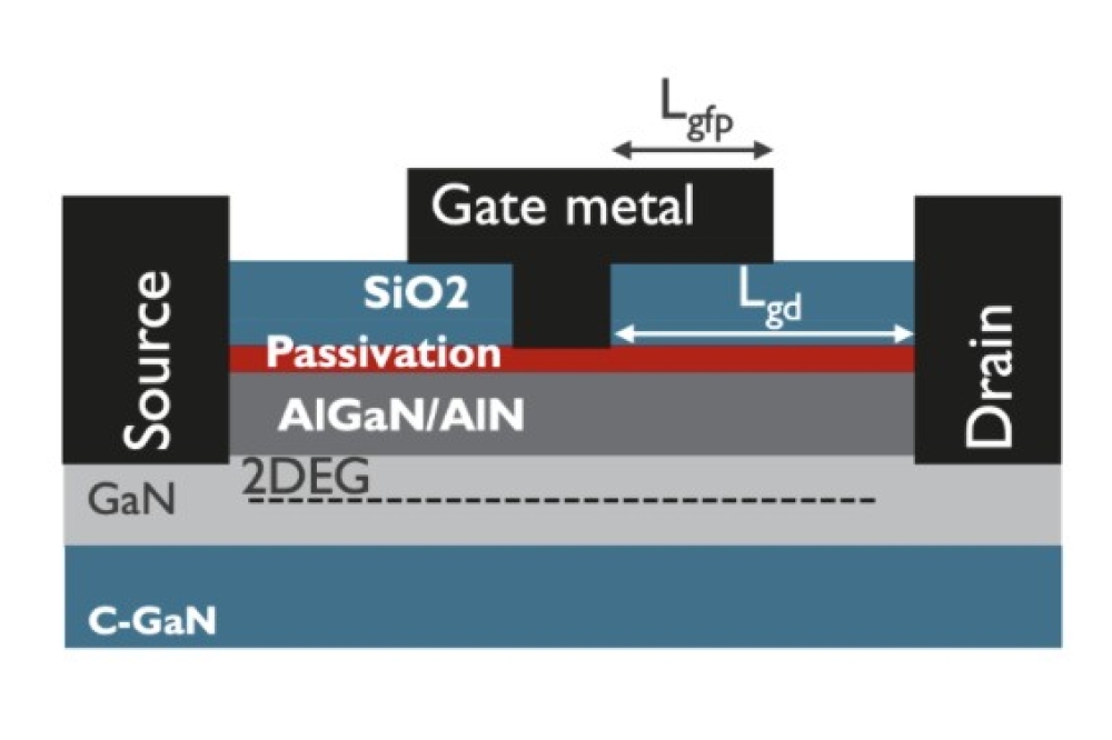
To suppress short channel effects, we employ a gate recess technology. Plots of transfer characteristics, involving measurements of the drive current as a function of the gate-source voltage, provide proof of great gate control, with a subthreshold swing of 160 mV/dec and a transconductance of 70 mS mm-1 (see Figure 3). Incorporating a T-gate field plate aids electric field management, with a β-Ga2O3 RF power device with a gate length of 180 nm and a gate-to-drain distance of 0.7 μm realising a breakdown voltage of 150 V – that translates to an average electric field of 2.15 MV cm-1. We have used TCAD simulations of the electric field to assess our device design. These simulations show that our T-gate field plate suppresses the peak electric field at the gate edge. Extracted peak electric fields in the β-Ga2O3 channel and SiC substrate are 8 MV cm-1 and 3 MV cm-1, respectively, suggesting a full exploitation of the high critical field of these materials (see Figure 4).
For RF power transistors, the output power under high-voltage operation can be pegged back by current collapse. It is generally accepted that this occurs when carriers are captured by traps, either at the interface or present in bulk material. We have investigated if current collapse is an issue in our devices by undertaking pulsed measurement at various quiescent bias points. Our measurements show minimal current collapse (see Figure 5). Compared with the DC curve, all the pulsed maximum drain currents are only slightly higher, even at a high drain-source voltage of 20 V. This lack of variation is evidence of excellent heat dissipation from the high-thermal-conductivity SiC substrate. Another encouraging result is that compared with the cold channel state, gate and drain pulsed on-current show no obvious change. The lack of current collapse verifies the high quality of our MOS interface and our β-Ga2O3 materials, which provide the foundation for realising a high output power and a high power-added efficiency at a high drain-source voltage.
Figure 6. (a) Small-signal RF performance of the β-Ga2O3 RF power FET with a gate length of 180 nm. Extracted fT (b) and fmax (c) dependence on the VGS and VDS mapping contour.
Drawing on great DC characteristics and a high-quality β-Ga2O3-on-SiC material platform, our β-Ga2O3 RF devices have values for fT and fmax of 27.6 GHz and 57 GHz, respectively. Additional impressive results are a value of around 5 GHz µm for the product of fT and the gate length, and 39.7 GHz for (fT×fmax)0.5. We find that the values for fT and fmax increase with drain-source voltage, due to an increased electric field along the channel that boosts carrier velocity. This trend is beneficial, as operating a power amplifier at a higher drain-source voltage increases its gain (see Figure 6).
Measurements of our device’s large-signal load pull characteristics using an input signal under continuous-wave mode show that introducing the β-Ga2O3-on-SiC material platform and a highly-doped β-Ga2O3 channel enables an output power density of more than 2.3 W/mm, realised with a power-added efficiency of 30 percent at 2 GHz (see Figure 7(a)). Output power density increases by 0.5 W mm-1 for every 5 V increase in the drain-source voltage (see Figure 7(b)).
Our efforts have included an expansion of the signal amplification range from 2 GHz to 8 GHz, with an output power density of almost 1 W mm-1 realised at 8 GHz. Note that this is the first demonstration of an oxide semiconductor RF power FET amplifying a signal of up to 8 GHz (see Figure 7(c)).
Figure 7. (a) Continuous-wave large-signal class-AB performance of the device with a power sweep at 2 GHz. (b) Output power (P out) and power-added efficiency (PAE) dependence on the drain-source voltage(V DS). (c) 8 GHz large-signal performance of the β-Ga2O3 RF power FET.
A key conclusion from our work to date is that high-voltage β-Ga2O3 RF power devices can operate at a high frequency with a high power density. Through innovation – the combination of a β-Ga2O3-on-SiC material platform, a highly-doped β-Ga2O3 channel, and a T-gate with field plate – we are concurrently realising efficient heat extraction, a low on-resistance, a high maximum drain current, a high blocking voltage, and high values for fT and fmax.
Our results verify the great promise of β-Ga2O3-on-SiC RF FETs for future high-voltage, high-frequency, high-power and high-efficiency applications. Our next steps are to optimise the fabrication process, scale the gate length, and produce hundreds-volt-class β-Ga2O3 RF devices.


















.jpeg)


