Axus secures $12.5M investment funding
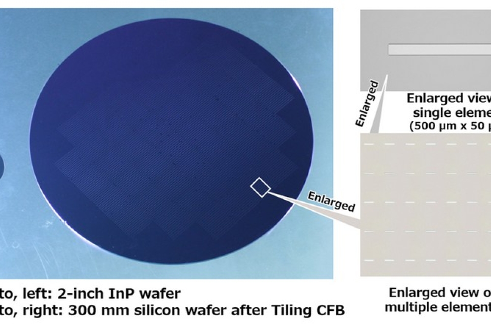
Company to use funds for expansion of CMP products for SiC device manufacturing
Axus Technology, an established US provider of chemical mechanical planarisation (CMP) equipment used for manufacturing compound semiconductors, has received $12.5 million in capital funding from firm IntrinSiC Investment LLC. In addition, the company has secured a significant line of credit from a national US bank.
Axus Technology is looking to use the funds to drive higher volume sales and enter new markets with its CMP processing tools.
“We are thrilled to partner with IntrinSiC Investment to secure funding that supports our expansion. With this additional funding, we are strongly positioned to support our rapidly growing installed base of high-performance Capstone CMP systems, particularly with our leading-edge, high-volume customers,” said Axus Technology CEO Dan Trojan.
“In addition to strengthening our balance sheet, we expect to significantly benefit from the interaction, support and contribution of IntrinSiC’s principals, whose skill and experience in the semiconductor industry and impressive track record will greatly benefit Axus Technology’s continued growth and evolution.”
Johannes Froehling, general partner, IntrinSiC Investment, said:, “We have been engaged in the compound semiconductor ecosystem for more than a decade. Over the past two years, we have made strategic investments in companies with a strong focus on SiC, as well as gallium nitride, or GaN. Our approach is to seek recommendations from leading chipmakers for companies with a solid, technically differentiated product portfolio that are well positioned to move to high-volume manufacturing once capitalised. Axus Technology was cited across the board as a company that met or exceeded these characteristics. We’re excited to play a role in enabling the next phase of their success.”