Improving HEMT reliability with oxygen plasma treatment
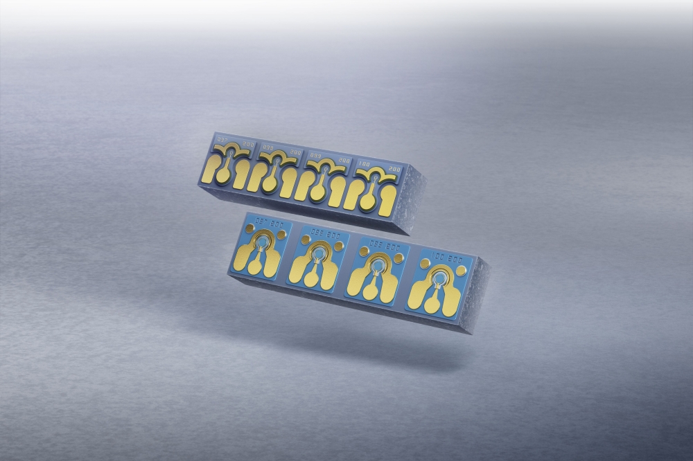
Engineers from China are claiming to have developed a simple, low-cost approach based on oxygen plasma treatment to improve the reliability of p-GaN gate HEMTs.
According to these researchers from Southern University of Science and Technology, their process extends the lifetime of Schottky-type p-GaN HEMTs by reducing the electric field in this device through compensation of magnesium acceptors.
This breakthrough could strengthen the competitiveness of Schottky-type p-GaN HEMTs, which offer excellent electrical efficiency and are already winning deployment in a number of applications, including data centres, electric vehicles and consumer electronics.
Today’s commercial Schottky-type p-GaN HEMTs suppress gate leakage, but are hampered by a narrow bias window for safe operation that stems from the time-dependent gate breakdown. Catastrophic breakdown results from degradation at the metal/p-GaN Schottky junction, caused by a combination of hot electron bombardment and electric field stress.
Several teams have devised ways to slow this degradation, by either increasing the robustness to hot electron bombardment or reducing the electric field strength. Introducing materials such as GaON, Ga2O3 and AlGaN combat electron bombardment, and the addition of an intrinsic GaN layer quashes the electric field strength. However, these approaches either require: the growth of new layers on the p-GaN surface, leading to concerns related to the magnesium memory effect; or high-temperature annealing, which adds to the thermal budget.
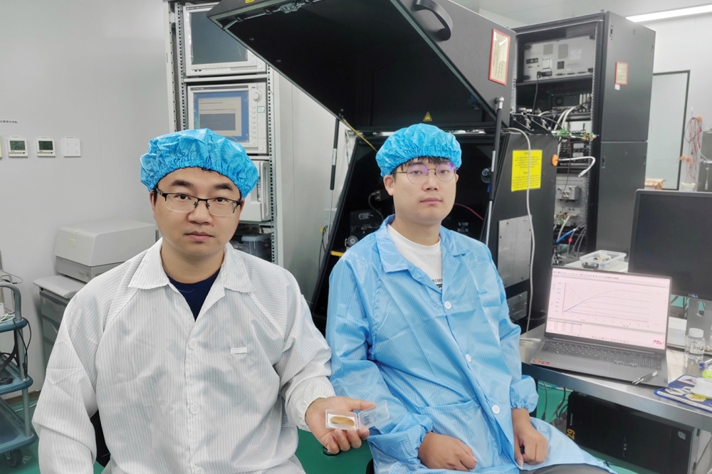
Addressing all these concerns is the process developed by engineers from Southern University of Science and Technology. According to spokesman Chengcai Wang, their team’s approach has been inspired by the work of Kevin Chen’s group from The Hong Kong University of Science and Technology – that team employed oxygen plasma treatment to deplete the top layer of p-GaN and obtain a normally-off p-FET. Wang says that based on that finding, he and his co-workers thought that oxygen plasma treatment might offer a simple and effective method to compensate for magnesium on the p-GaN gate surface and thus reduce the peak electric field.
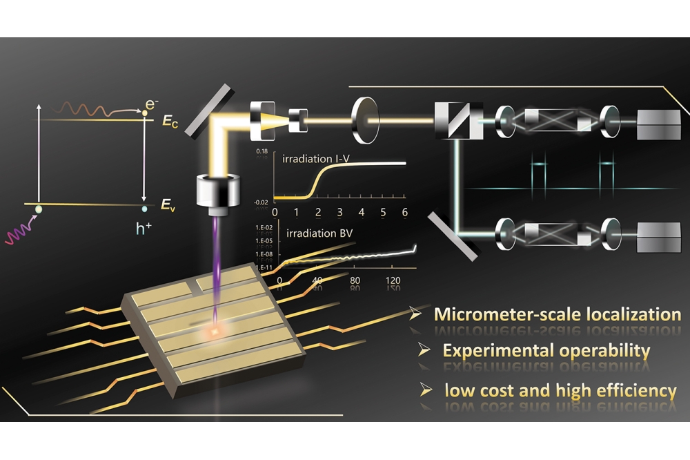
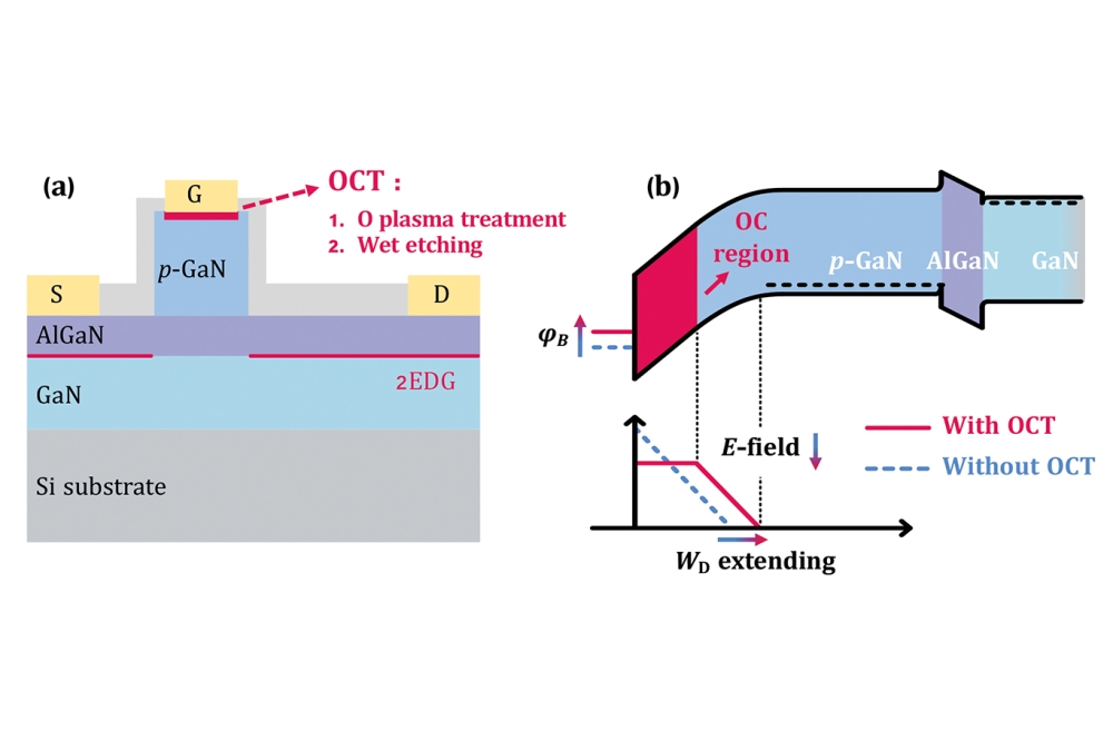
To investigate this possibility, Wang and co-workers have used oxygen plasma treatment when producing devices. Oxygen penetrates into the p-GaN layer to form oxygen donors or MgO complexes that compensate for the activated magnesium dopants. A weakly doped or intrinsically doped GaN layer results, decreasing the local electric field (see figure).
According to Wang, oxygen treatment has the potential to be employed for high-volume production, because it avoids complicated equipment and the entire process is compatible with the current GaN manufacturing process. “Furthermore, a uniform oxygen plasma is usually easy to obtain,” claims Wang.
The team fabricated its HEMTs by removing the p-GaN stack outside the gate region, adding source and drain contacts, undertaking planar isolation and depositing a passivation layer. After plasma treatment, soaking the sample in HCl removed the regions of the p-GaN layer that were heavily oxidised or damaged, prior to the addition of a Ni/Au gate contact, annealed at just 350 °C.
Comparing the characteristics of plasma-treated and untreated HEMTs revealed that the introduction of oxygen reduced the leakage current and capacitance of the Schottky junction. Additional benefits included an increase in the room-temperature breakdown voltage from 10.4 V to 14.5 V, and an increase in the time-dependent gate breakdown. Evidence of the latter is an increase in the maximum bias from 4 V to 8.1 V, for a 1 percent failure rate for a 10-year lifetime.
“In future work, we plan to more comprehensively study the effect of oxygen plasma treatment process parameters on device performance and improve the effect of oxygen compensation technology in practical applications,” said Wang.
Reference
C. Wang et al. Appl. Phys. Express 17 051002 (2024)

