Raising the bar for β-Ga₂O₃ diodes
Heterojunction barrier Schottky diodes combine a low turn-on voltage with a high breakdown
To unleash the potential increase in rectifier efficiency with β-Ga2O3 diodes, these devices need to combine a lower turn-on voltage and a diminished on-resistance with superior suppression of the reverse leakage current.
Addressing this challenge is a team from the University of Science and Technology of China that has unveiled a β-Ga2O3 heterojunction barrier Schottky diode equipped with a tungsten Schottky contact.
According to team spokesperson Quiyan Li, the most significant breakthrough associated with their recent work is the validation that a low-work-function metal leads to a low Schottky barrier height for β-Ga2O3, significantly reducing the turn-on voltage of these devices.
Typically, β-Ga2O3 diodes employ high-work-function metals for Schottky contacts, such as nickel and platinum, resulting in a turn-on voltage of 0.8 V. And even higher values of up to 2 V are realised when metal oxides, such as PtOx and NiO, are introduced to trim the reverse leakage current. In stark contrast, the diodes made by Li and co-workers, featuring a tungsten Schottky contact, have a turn-on voltage of just 0.48 V.
Another important aspect of the devices pioneered by Li and co-workers is the use of p-type NiO to supress the reverse leakage current.
“As a result, we fabricated a unipolar diode with a breakdown voltage exceeding 1.3 kV,” says Li.

To quantify the capabilities of this particular design, Li and co-workers evaluated the performance of heterojunction barrier Schottky diodes, Schottky barrier diodes, and heterojunction diodes. All three were fabricated from epiwafers purchased from Novel Crystal Technology that contained a 10 µm-thick, lightly-doped β-Ga2O3 layer grown by HVPE.
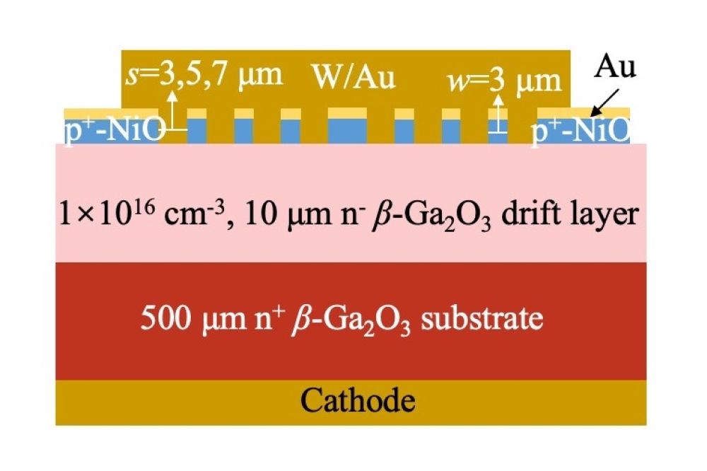
Production of devices from the HVPE-grown epiwafer began by chemical cleaning the surface and adding a Ti/Al/Ni/Au contact to the backside of the wafer. Formation of the top contact included using lithography to define spacer widths, and sputtering to deposit heavily-doped regions of 220 nm-thick NiO coated with 50 nm-thick gold.
To form the anode, the team added a 50 nm-thick layer of tungsten and a 150 nm-thick layer of gold (see Figure for the resulting device architecture).
Measurements of the on-voltage, determined for a forward current density of 100 mA cm-2, provided a value of 0.48 V for the heterojunction barrier Schottky diode, compared with 0.46 V for the Schottky barrier diode and 2.04 V for the heterojunction diode. For the heterojunction barrier Schottky diode, the forward-current density increases at a faster rate for voltages beyond the turn-on voltage for the heterojunction diode, thanks to a switch to bipolar operation.
The breakdown voltage of the heterojunction barrier Schottky diodes is 1558 V, significantly higher than that for the Schottky barrier diode and heterojunction diode, which have values for this key metric of 756 V and 1347 V, respectively. However, even the heterojunction barrier Schottky diode breaks down at a field strength of 2.46 MV cm-1, far short of the maximum field strength for β-Ga2O3 of 8 MV cm-1.
One of the next goals for Li and co-workers is to employ an embedded NiO for the junction barrier Schottky structure with stronger depletion capability to suppress the reverse leakage current. “However, this structure will bring challenges in repairing sidewall etching damage,” says Li.
“After that, we will further optimise the parameters of the epitaxial layer, such as adopting a double-layer drift layer, in order to achieve low on-resistance while maintaining low surface electric field, low reverse leakage, and good breakdown capability.”
Reference
Q. Li et al. Appl. Phys. Express 17 066501 (2024)
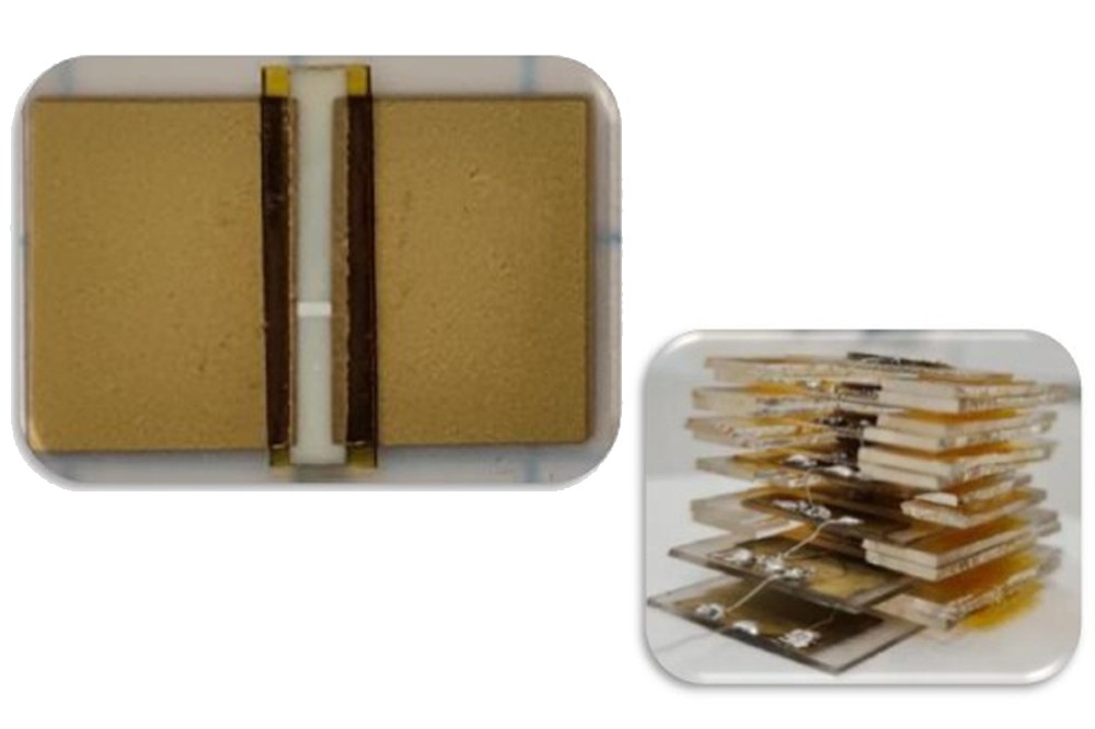
Main image:Heterojunction barrier Schottky diodes almost match Schottky diodes for turn-on characteristics, while providing the highest breakdown voltages.