Wet chemical etching for defect-free AlGaInP red micro-LEDs
A key challenge in commercialising high-resolution micro-LED displays is reducing LED chip size without losing efficiency, especially for the phosphide-based red micro-LED, which is more vulnerable to efficiency drop than blue and green devices.
The main reason for the micro-LED efficiency drop is the chip sidewall defects generated by energetic plasma during the mesa dry etching. Nevertheless, there have been no reliable options to replace the dry etching up to now.
As a result, most efforts have been focused on the post dry etching recovery, such as chemical treatment, annealing, and passivation deposition. However, they are helpful for partial recovery only. More importantly, they are not effective for tiny chips used for high resolution displays because sidewall defect penetration depth is close to or in excess of the micro-LED chip dimension.
As a result, 'defect-free' etching approaches have been sought for a long time.
Wet etching is promising as it is 'defect-free', but the isotropic etching characteristic leads to detrimental undercut. For this reason, wet etching has been perceived not suitable to etch small chips like micro-LEDs.
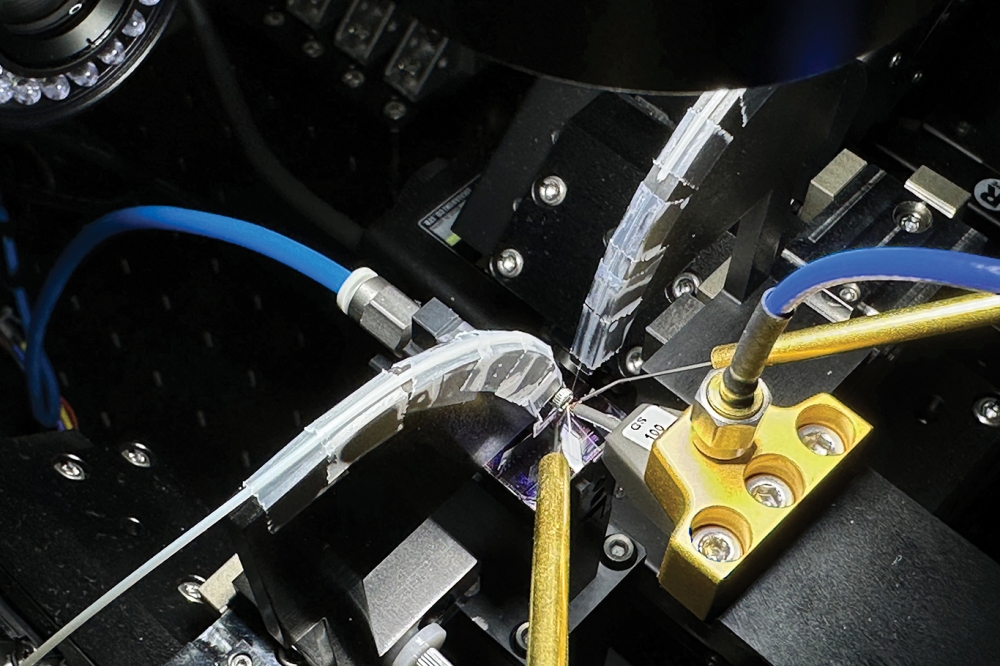
Recently, Verticle, a San Francisco-based firm specialising in the development of LEDs and related displays, has reported a breakthrough in a method of mesa etching of AlGaInP native red micro-LEDs by 'defect-free' wet chemical etching.
According to Mike Yoo, Verticle's CEO, the company is ready to apply this wet etching technology to mass production of AlGaInP red micro-LEDs to accelerate the commercialisation of entire micro-LED displays from large screen to near eye displays.
Comparing sidewall defect penetration depth and effective mesa area
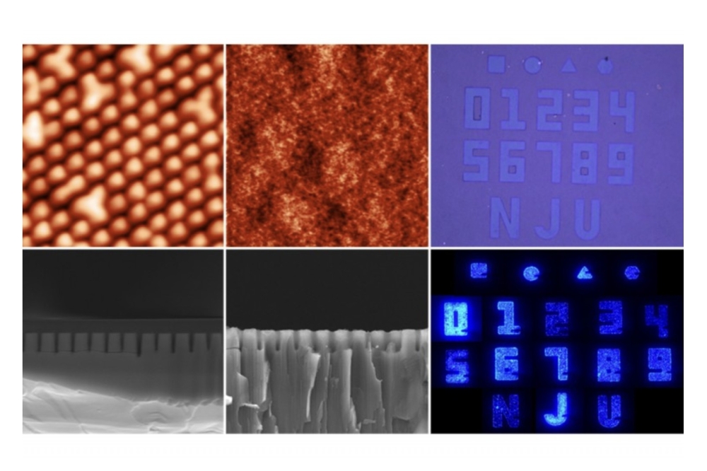
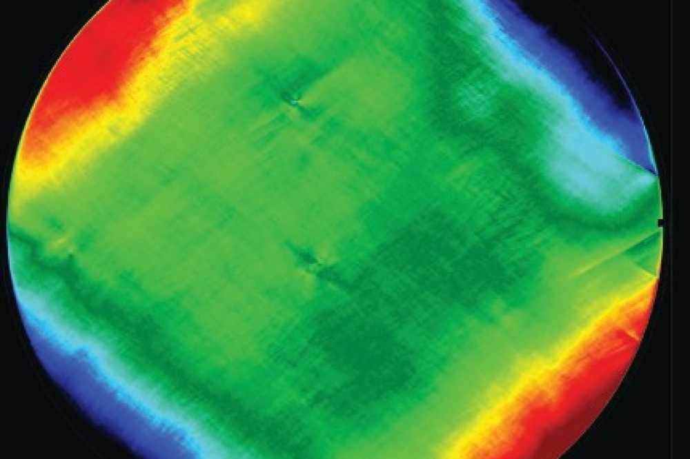
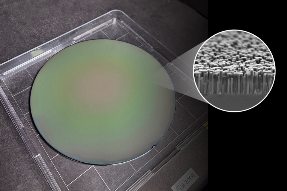
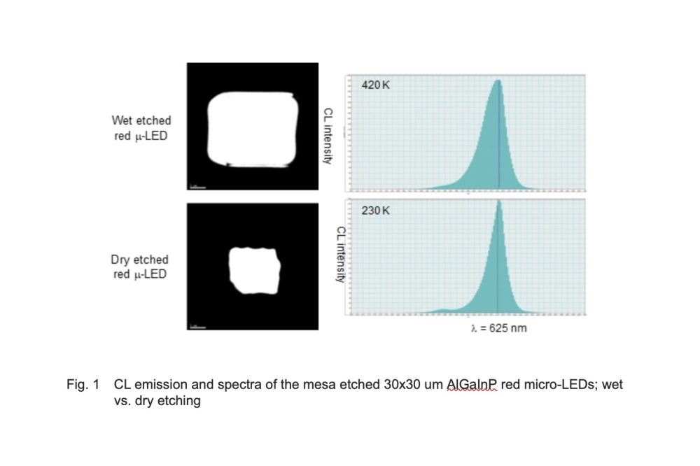
Sidewall defects in wet and dry etched AlGaInP red micro-LEDs are observed and compared using Cathodoluminescence (CL). During CL operation, an electron beam bombards the micro-LED surface and produces electron-hole pairs. Radiative recombination takes place from the electron-hole pairs in the undamaged crystal, as a result, bright emission images can be obtained. In contrast, non-radiative recombination takes place in the damaged crystal, thus little or no luminescence from the damaged portion of the micro-LED.
CL emission images and spectra in Fig. 1 above show clear difference between the wet and dry etched AlGaInP red micro-LEDs. CL emission from the wet etched micro-LED is significantly brighter and more than three times bigger than that of the dry etched, according Mike Yoo.
In particular, the sidewall defect penetration depth of the dry etched micro-LED is ~7µm, while almost no or less than 0.2 µm for the wet etched micro-LED (Fig. 2 below). Accordingly, effective mesa area of the dry etched red micro-LED is only 28 percent of the wet etched. The CL results, says Yoo, show that there are almost no or negligible number of defects exist in the wet etched AlGaInP red micro-LED.

These results, says Yoo, indicate that there is a distinct etching mechanism difference between wet and dry etching. Wet etching removes material by chemical reaction, thus no defects are formed, whereas dry etching physically removes material by energetic plasma that causes defect generation on the chip sidewall.
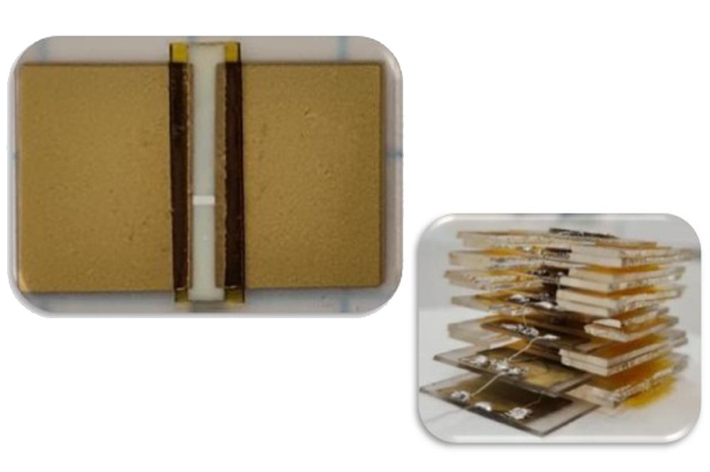
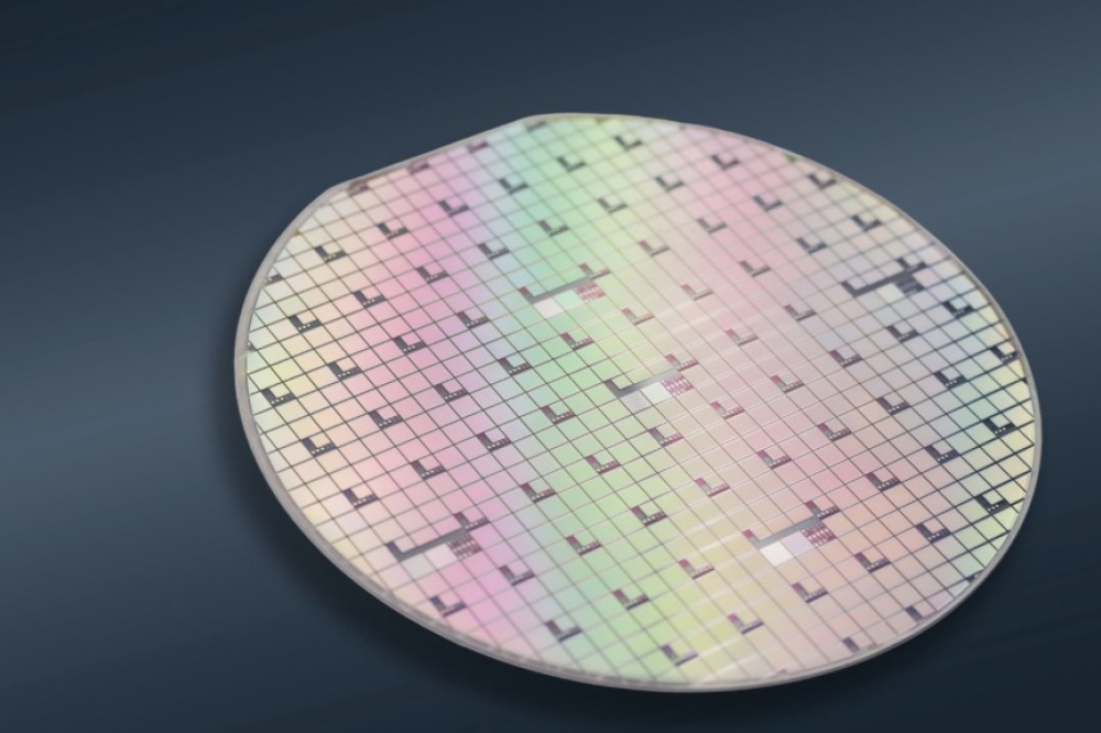
Besides the performance enhancement, cost benefits are huge with wet etching, adds Yoo. Unlike single wafer process in the case of dry etching (for over 6-inch wafer), wet etching is capable to etch multiple large diameter wafers in one batch that results in massively high throughput.
Furthermore, wet etching capital investment is incomparably lower than that of dry etching as no multiple number of extra high cost process tools, such as ICP RIE, ALD are needed.