Technique offers fast, large-area deposition of 2D films
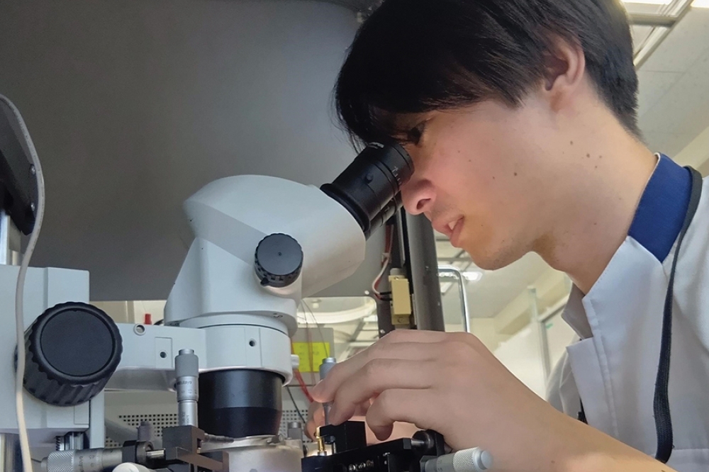
A Japanese research team led by Minoru Osada, a professor from the Institute for Materials and Systems for Sustainability (IMaSS) at Nagoya University has pioneered a method for the high-speed, large-area deposition of 2D materials, including oxides, graphene oxide, and the compound semiconductor boron nitride.
The technique, known as the ‘spontaneous integrated transfer method’, was discovered by chance. The team thinks it could revolutionise the production of nanosheets. The research findings were published in the journal Small.
Traditionally, methods like CVD and the Langmuir-Blodgett (LB) technique have been employed for nanosheet fabrication. However, these methods have significant obstacles to their use, including difficulties in achieving uniform, large-area deposition and complications in the substrate transfer process.
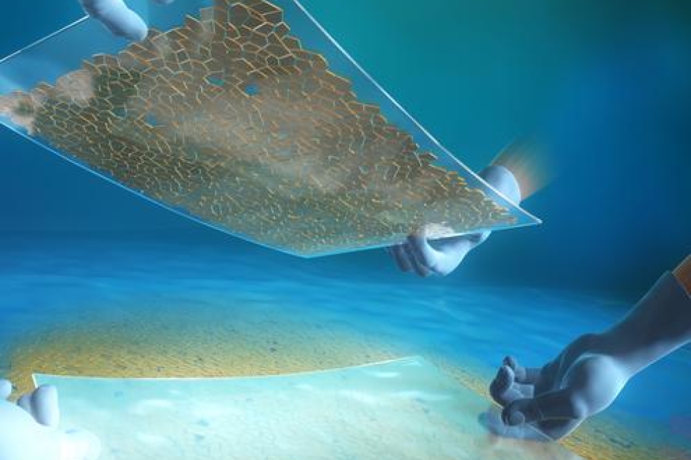
But Osada’s team discovered a fascinating phenomenon completely by chance: when nanosheets got wet, they spontaneously align themselves on the surface of water, forming dense films within a mere 15 seconds. This process, termed the ‘spontaneous spreading phenomenon’, suggested a more effective deposition technology.
The group tested this technique by dropping a nanosheet solvent mixture onto the water surface. Due to ethanol’s higher volatility compared to water, it evaporates more rapidly, creating a concentration gradient at the surface. Regions with more ethanol evaporation have higher surface tension than those with higher ethanol concentration. This difference in surface tension causes fluid to move from areas of lower to higher tension, generating convection currents. These currents guide the nanosheets within the solution, causing them to arrange in a more ordered and dense formation on the water surface.
“The nanosheets spontaneously align and pack closely together, much like ice floes coming together on the surface of water,” Osada said. “This controlled alignment is essential for creating uniform and high-quality nanosheet films. The resulting nanosheet film can then be easily transferred onto a substrate, completing the deposition process in as little as one minute.”
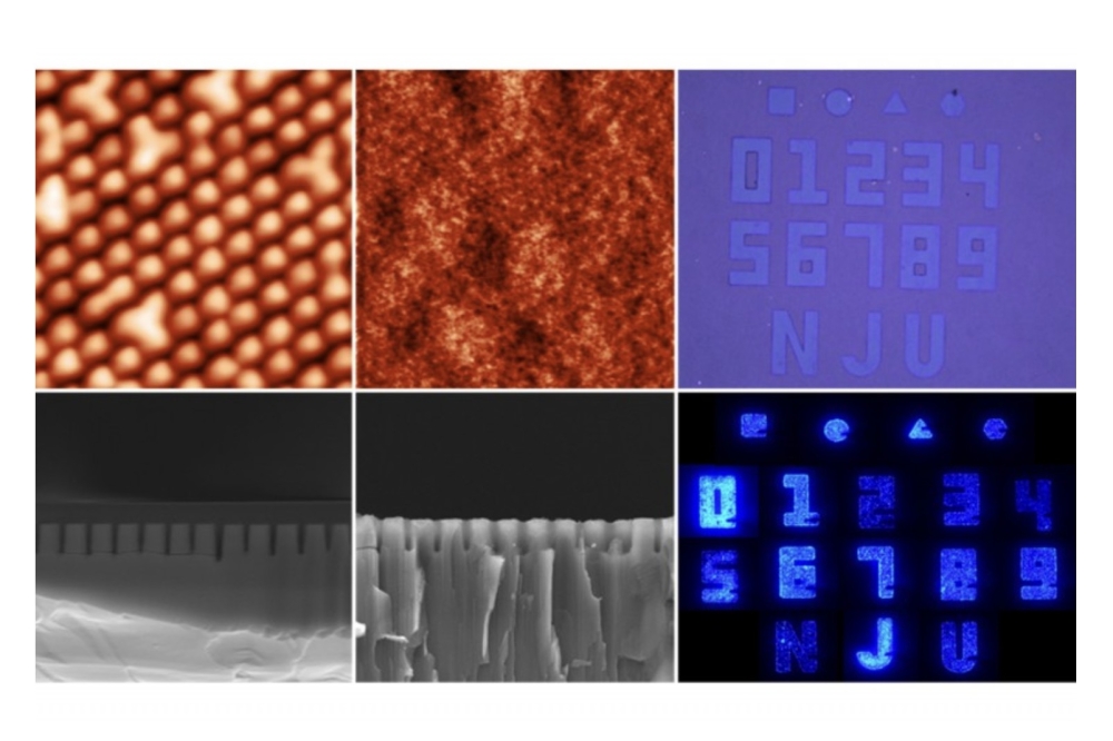
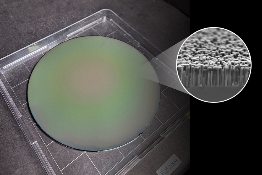
This method not only simplifies the production process but also opens the door to producing multilayer thick films with 100 to 200 layers—something that has been difficult to achieve with conventional methods like CVD and LB. Atomic force microscopy and confocal laser microscopy confirmed that the nanosheet films produced through this technique were highly uniform, with densely packed nanosheets arranged like pieces of a jigsaw puzzle.
The group were surprised by the versatility of this technique, applying it successfully to various nanosheet compositions and structures, allowing for the production of large-area films on substrates of different shapes and materials.
"The multilayer films fabricated by this technology exhibit excellent properties as functional thin films. They could be used in transparent conductive films, dielectric films, photocatalytic films, corrosion prevention films, and thermal shielding films," Osada said.
In addition to its technological advantages, Osada emphasised the environmental benefits of this method: "This technology is expected to become an important environmentally friendly eco-process because it enables thin film production on various substrates at room temperature and in an aqueous solution process, without the need for vacuum film-forming equipment or expensive tools, which are common in conventional thin film processes."