Irradiation-hardened GaN HEMTs
A collaboration between engineers at Nanjing University and CorEnergy Semiconductor is claiming to have broken new ground by demonstrating robust radiation hardness in novel p-GaN HEMTs.
According to team spokesman Feng Zhou from Nanjing University, this triumph could open up new and lucrative markets for the GaN HEMT. “We believe that GaN devices have a very broad market in radiation environments, which could reach hundreds of millions of US dollars or more,” argues Zhou, who claims that there is an urgent need for advanced wide bandgap semiconductors in orbital satellites, spacecraft, and weapons facilities.
To demonstrate the superior radiation hardness of their p-GaN HEMTs, which remove holes accumulated under radiation, Zhou and co-workers have benchmarked their devices against conventional GaN HEMTs using the value for single-event burnout at a linear energy transfer of around 78 MeV cm2 mg-1. Linear energy transfer is the average radiation energy deposited per unit path length along the track of an ionizing particle.
“The linear energy transfer describes the energy-deposition density of a particular type of radiation, which largely determines the adverse consequence of radiation exposure, such as degradation of electrical properties and radiation damage,” explains Zhou.
For the team’s p-GaN HEMTs, single-event burnout at a linear energy transfer of around 78 MeV cm2 mg-1 occurs at 558 V. In stark comparison, typical GaN HEMTs have values of between 100 V and 200 V.
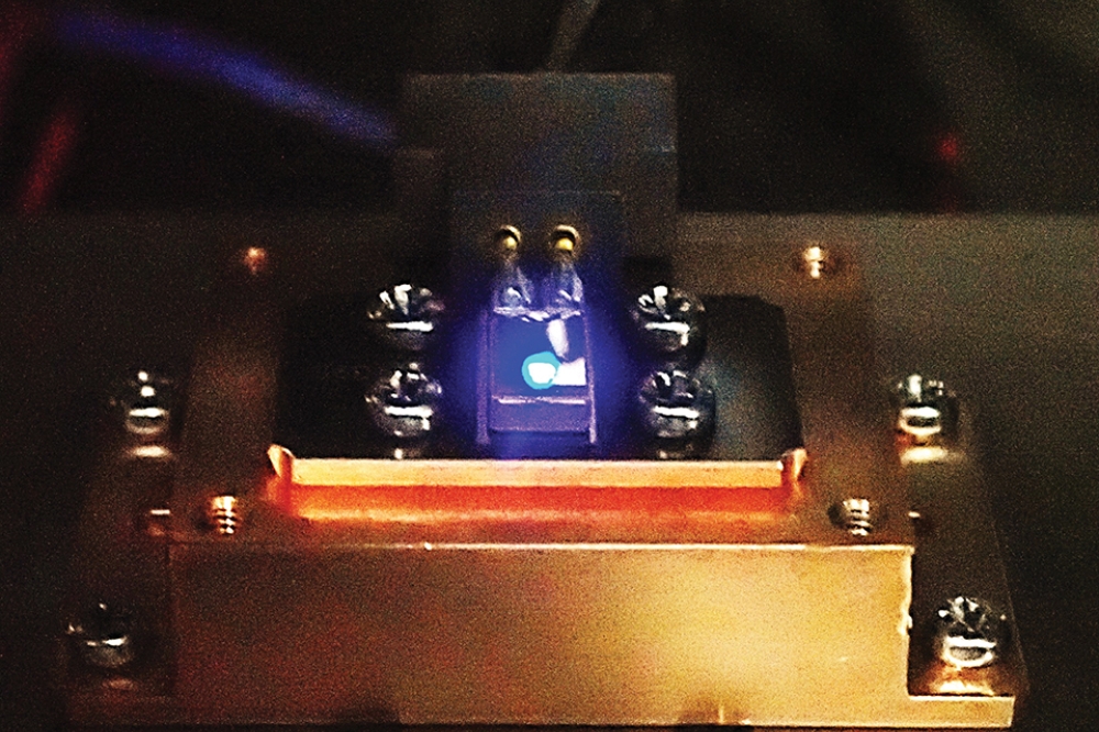
Another important aspect of the work of Zhou and colleagues is the development of an ultraviolet pulsed laser irradiation system that enables the evaluation of the dynamic characteristics of devices through integrated power switching circuits. According to Zhou, this novel alternative to a heavy-ion accelerator has enabled the first measurements that assess the power-conversion efficiency of GaN power devices under radiation.
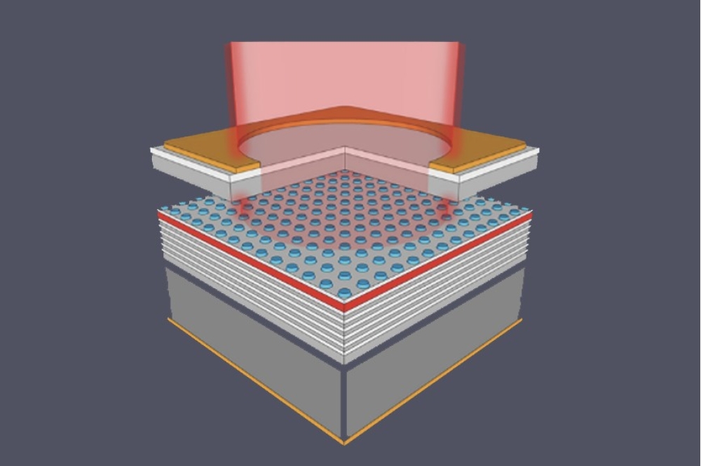
Prior to the fabrication of their p-GaN HEMTs, Zhou and co-workers modelled the conventional form of this device. They found that radiation-induced holes accumulate in the channel/buffer regions near the gate stack, due to the reverse blocking of the p-i-n junction, which is composed of p-GaN/AlGaN/GaN in the gate stack of the p-GaN HEMT.
Based on this insight, the team introduced a partitioned design of the gate stack that safely dissipates accumulated holes and improves tolerance to single-electron burnout.
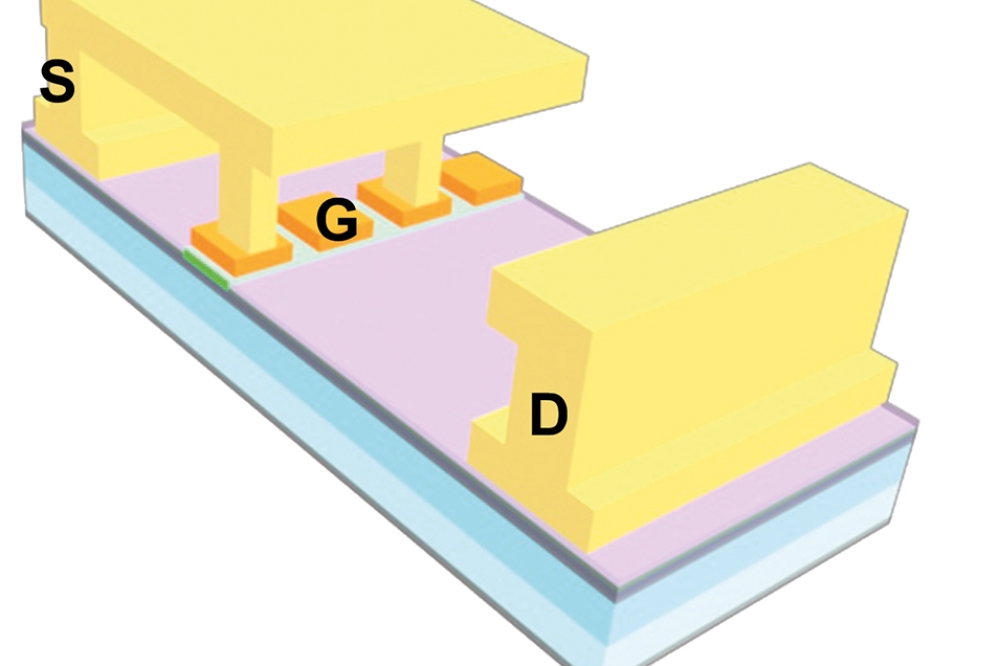
Their novel HEMT architecture is realised by patterning the gate metal layer that’s deposited on the p-GaN layer into segments, enabling some of the spaced metal fingers to no longer serve as gate electrodes, but be connected to the source metal via a field-plate interconnect process. Another departure from the norm is the etching of the middle region of p-GaN beneath the source-connected metals, so that these metals can be deposited directly on top of the AlGaN layer to form an ohmic contact. With this approach, the source-connected-metal/AlGaN/GaN ohmic contact contributes to the dissipation of holes.
Electrical measurements, comparing the radiation-hard HEMT with a control, reveal that the former has a higher threshold voltage and on-resistance – 3.3 V, rather than 3.0 V; and 223 mΩ, compared with 188 mΩ. Both increases are attributed to the source-connected buried metal structure that occupies part of the original gate region and weakens the current conduction capability.
Heavy-ion accelerator-based irradiation experiments using linear energy transfers of around 76 MeV cm2 mg-1 and 86 MeV cm2 mg-1 led to average values for the single-event burnout voltages of 558 V and 467 V, respectively, for the radiation-hard HEMT. In comparison, the equivalent values for the conventional HEMT were just 217 V and 89 V, respectively.
Operating under laser irradiation, a 300 W power factor conversion system has been found to have an efficiency of 95 percent under a linear energy transfer of around 76 MeV cm2 mg-1, compared with 91 percent for an equivalent system featuring a radiation-hardened 400 V vertical double-diffusion silicon MOSFET.
Zhou says that the next goal is to apply their radiation-hardened devices to circuit systems and conduct application verification for aerospace electronic systems.
Reference
F. Zhou et al. IEEE Electron Dev. Lett 45 976 (2024)