Element Six to lead DARPA UWB program
Element Six, part of the De Beers Group, will lead a US Defense Advanced Research Projects Agency (DARPA) program to develop advanced UWBG (ultra-wide banddap) semiconductors.
The goal is to develop UWBG substrates, device layers, and junctions, for next generation electronics, including high-power RF switches, amplifiers for radar and communications, high-voltage power switches, high-temperature electronics for extreme environments, and deep UV LEDs and lasers.
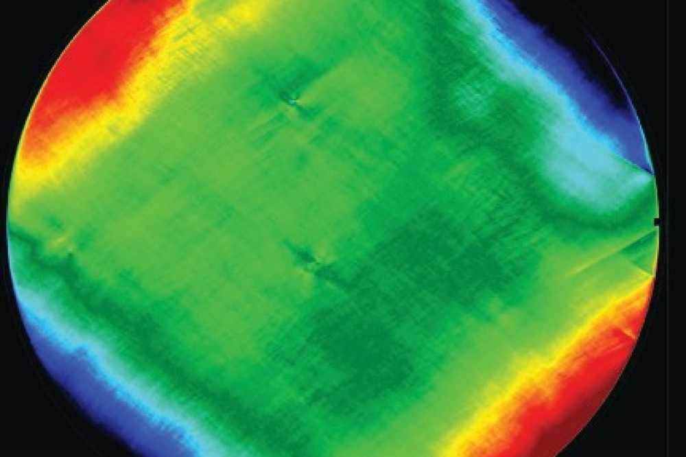
E6's contribution will harness the company's expertise in large area CVD polycrystalline diamond and high-quality single crystal (SC) diamond synthesis, to realise 4-inch device grade SC diamond substrates.
E6 will be partnering with Orbray in Japan (with diamond heteroepitaxy expertise), Raytheon (leaders in GaN RF devices), Hiqute Diamond in France (with dislocation engineering expertise), and Stanford and Princeton Universities in the US (with materials bulk and surface processing characterisation expertise).
Daniel Twitchen, chief technologist at Element Six, said: "Industrial diamond has disrupted multiple markets since its first scale synthesis in the 1950s, and I am confident that technology breakthroughs in UWBGS will help unlock another 70 years of positive disruption in the semiconductor industry."
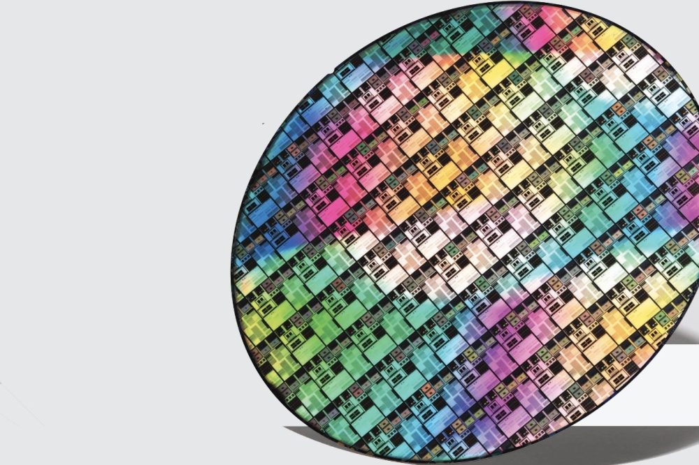
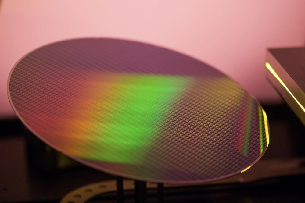
E6 polycrystalline diamond wafers over 4 inches in diameter are already enabling telecommunication infrastructures and defence applications, being used as either optical windows in EUV lithography for silicon chips, or in thermal management applications for high-power density silicon and GaN devices
E6 SC diamond was a crucial enabler in the CERN Large Hadron Collider's monitoring systems, helping lead to the discovery of the Higgs Boson Particle. In partnership with high-power semiconductor leader ABB, E6 realised the first high-voltage bulk diamond-based Schottky diodes. Furthermore, E6 recently completed build and commission of an advanced CVD facility using its core technology in Portland (OR), powered by renewable energy sources.

